
Package structure having MEMS elements and fabrication method thereof

a technology of microelectromechanical system and packaging structure, which is applied in the direction of fluid pressure measurement, instrumentation, and semiconductor/solid-state device details, can solve the problems of large size of packaging structure, high degree of accuracy, and high cost of tsv technology for forming through holes and recesses, so as to reduce equipment and fabrication costs, reduce the overall thickness and size of the package structure, and reduce the effect of at least one round of exposur

Active Publication Date: 2012-11-22
SILICONWARE PRECISION IND CO LTD
View PDF5 Cites 13 Cited by
  • Summary
  • Abstract
  • Description
  • Claims
  • Application Information

AI Technical Summary

Benefits of technology

[0012]The present invention eliminates the need to form through holes in a silicon substrate as in the prior art so as to reduce equipment and fabrication costs. Further, the plate does not cover the bonding wires but the MEMS elements, and portions of the bonding wires are removed so as to reduce the overall thickness and size of the package structure. Furthermore, instead of forming additional alignment keys on the bottom surface of the wafer, the present invention allows the second alignment keys to be viewed via the transparent bodies such that a common alignment device can be used for an alignment step required in forming metal traces or an RDL layer, thereby reducing at least one round of exposure, development and etch processes and avoiding the use of an expensive double-sided alignment device so as to reduce fabrication costs and time.

Problems solved by technology

However, such a package structure has a large size and cannot meet the demand for lighter, thinner and smaller electronic products.
However, the TSV technology for forming the through holes and recesses is costly and requires a high degree of accuracy, thus complicating the fabrication process and increasing the fabrication cost.

Method used


Image

  • Package structure having MEMS elements and fabrication method thereof
  • Package structure having MEMS elements and fabrication method thereof
  • Package structure having MEMS elements and fabrication method thereof

Examples


Embodiment Construction

[0016]The following illustrative embodiments are provided to illustrate the disclosure of the present invention and its advantages, these and other advantages and effects being apparent to those in the art after reading this specification.

[0017]It should be noted that the drawings are only for illustrative purposes and not intended to limit the present invention. Meanwhile, terms such as ‘up’, ‘down’, ‘a’ and so on are used as a matter of descriptive convenience and not intended to have any other significance or provide limitations for the present invention.

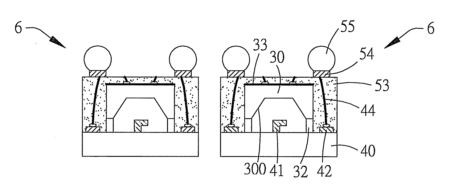
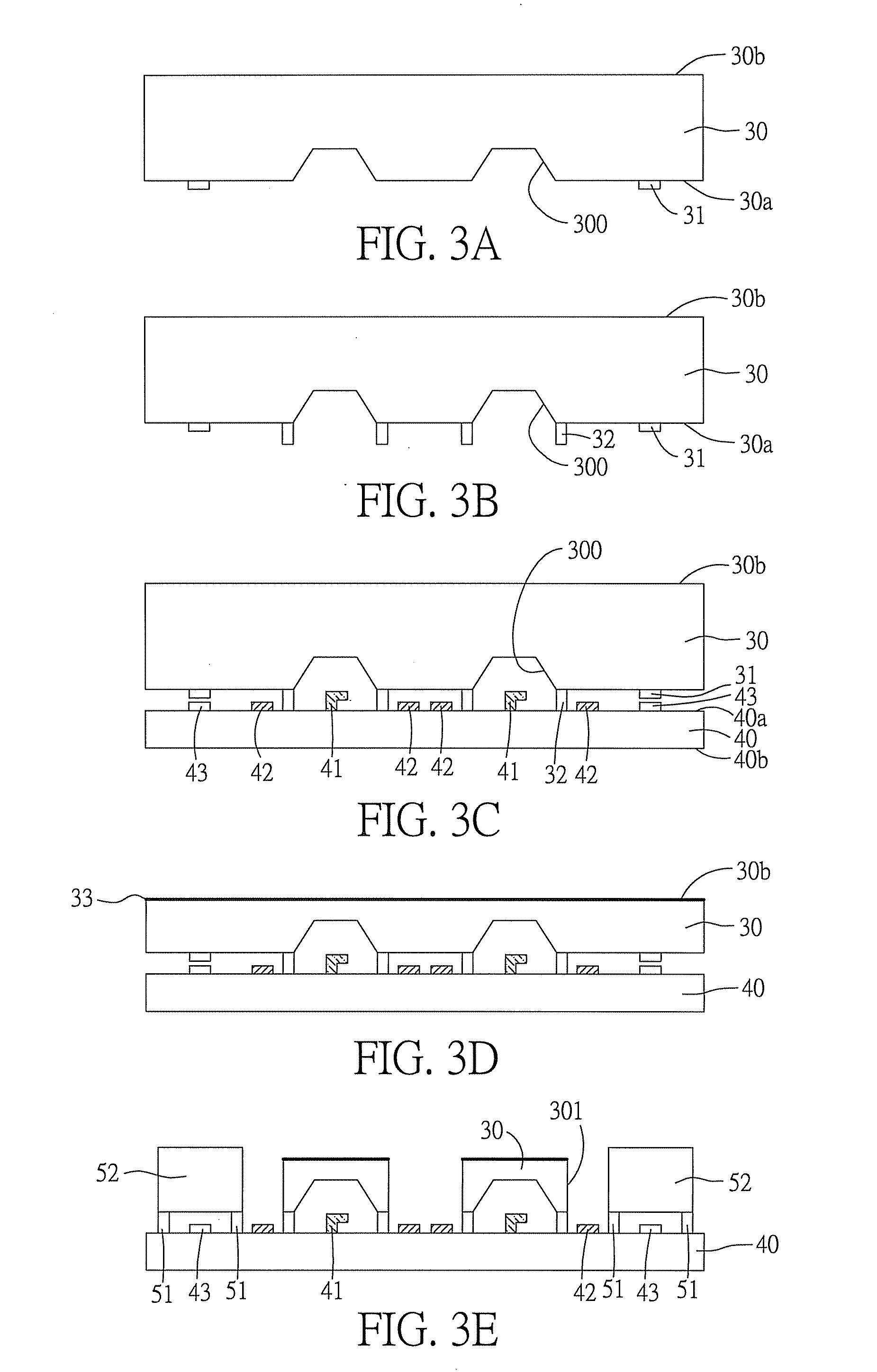
[0018]FIGS. 3A to 3K show a fabrication method of a package structure having MEMS elements according to the present invention. Therein, FIG. 3E′ is a top view of FIG. 3E, and FIG. 3J′ is another embodiment of FIG. 3J.

[0019]Referring to FIG. 3A, a plate 30 having a first surface 30a with a plurality of first alignment keys 31 and a second surface 30b opposite to the first surface 30a is provided. The plate 30 can be a silicon-cont...


PUM


Abstract

A package structure having MEMS elements includes: a wafer having MEMS elements, electrical contacts and second alignment keys; a plate disposed over the MEMS elements and packaged airtight; transparent bodies disposed over the second alignment keys via an adhesive; an encapsulant disposed on the wafer to encapsulate the plate, the electrical contacts and the transparent bodies; bonding wires embedded in the encapsulant and each having one end connecting a corresponding one of the electrical contacts and the other end exposed from a top surface of the encapsulant; and metal traces disposed on the encapsulant and electrically connected to the electrical contacts via the bonding wires. The present invention eliminates the need to form through holes in a silicon substrate as in the prior art so as to reduce fabrication costs. Further, the present invention accomplishes wiring processes by using a common alignment device to thereby reduce equipment costs.

Description

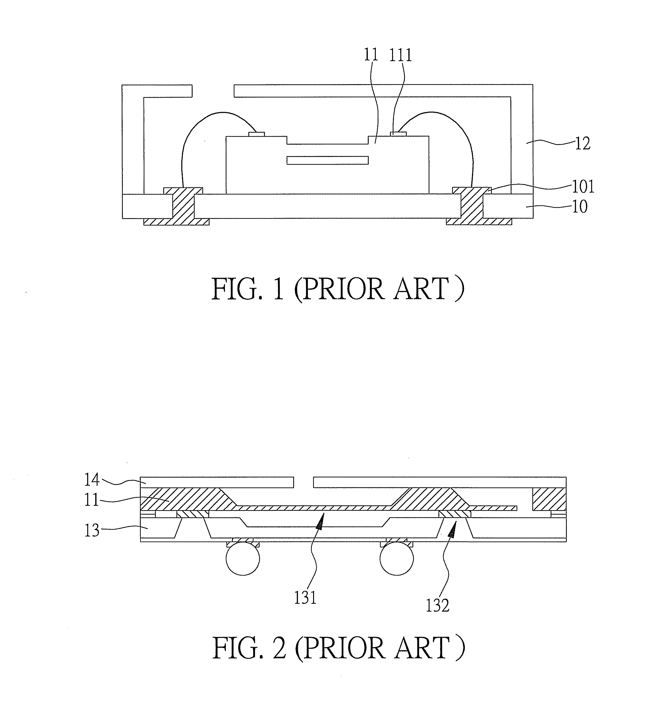
BACKGROUND OF THE INVENTION[0001]1. Field of the Invention[0002]The present invention relates to package structures, and, more particularly, to a package structure having MEMS (micro-electro-mechanical system) elements and a fabrication method thereof.[0003]2. Description of Related Art[0004]MEMS elements have integrated electrical and mechanical functions and can be fabricated via various micro-fabrication technologies. A MEMS element can be disposed on a substrate and covered by a shield or packaged with an underfill adhesive so as to form a MEMS package structure.[0005]FIG. 1 shows a cross-sectional view of a conventional package structure having a MEMS element. Referring to FIG. 1A, a MEMS element 11, such as a pressure sensing element, is disposed on an LGA (land grid array) substrate 10 and conductive pads 111 of the MEMS element 11 are electrically connected to conductive pads 101 of the LGA substrate 10 via a plurality of bonding wires. Further, a metal lid 12 is disposed on...

Claims


Application Information

Patent Timeline
IPC IPC(8): H01L29/84H01L31/0224H01L31/18H01L21/78H01L31/0203H01L21/56
CPCB81B7/007B81B2207/098B81C2203/054H01L2224/48091H01L2924/1461H01L2924/3025H01L2924/00014H01L2924/00H01L2924/16151H01L2924/16152
Inventor LIN, CHEN-HANCHANG, HONG-DALIAO, HSIN-YICHIU, SHIH-KUANG
Owner SILICONWARE PRECISION IND CO LTD
Learn More