Chip-scale package

a chip-scale and package technology, applied in the field of semiconductor package, can solve the problems of poor poor distribution of the build-up dielectric layer, etc., and achieve the effect of improving the reliability of the chip-scale packag

Inactive Publication Date: 2012-12-13
SILICONWARE PRECISION IND CO LTD
View PDF23 Cites 35 Cited by
  • Summary
  • Abstract
  • Description
  • Claims
  • Application Information

AI Technical Summary

Benefits of technology

[0012]It is known from the above that, in the chip-scale package according to the present invention, the buffering dielectric layer is used to replace the build-up dielectric layer. Since having a good non-wetting property with respect to the encapsulating layer, the buffering dielectric layer is evenly distributed on the encapsulating layer.
[0013]Moreover, the solvent in the buffering dielectric layer does not cause damages to the encapsulating layer, and the buffering dielectric layer is adhered to the encapsulating layer securely. Accordingly, delamination does not occur between the buffering dielectric layer and the encapsulating layer, and therefore reliability of the chip-scale package can be effectively improved.

Problems solved by technology

However, in the chip-scale package 1 the material of the build-up dielectric layer 12 suffers a non-wetting problem with respect to the material of the encapsulating layer 10, which results in a poor distribution of the build-up dielectric layer 12.
As a result, the build-up dielectric layer 12 is likely to be delaminated from the encapsulating layer 10 due to their poor adhering property, and the chip-scale package 1 thus has poor reliability.
Therefore, how to overcome the problems of the prior art is becoming one of the most imperative issues in the art.

Method used


Image

  • Chip-scale package
  • Chip-scale package
  • Chip-scale package

Examples


first embodiment

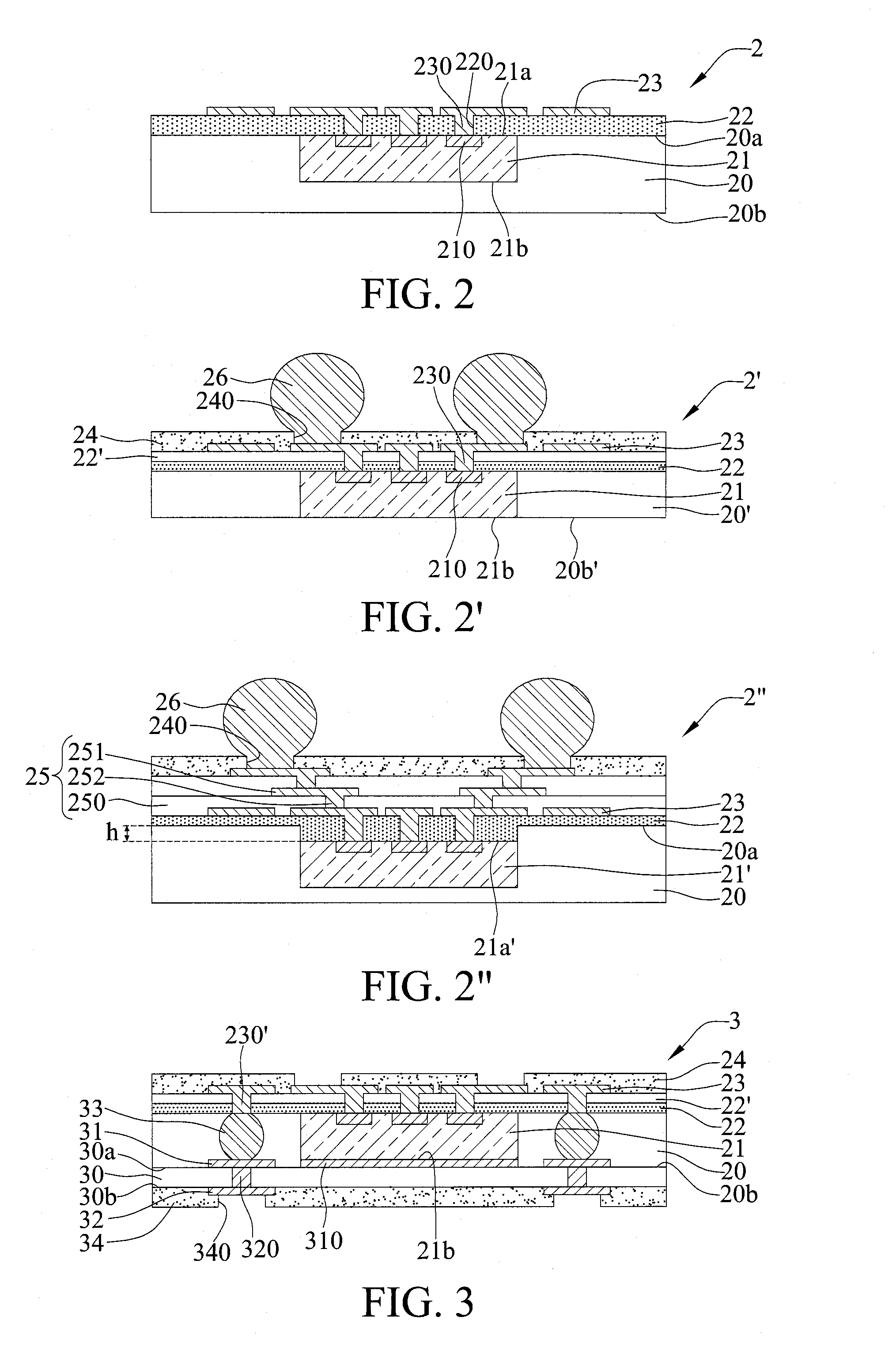
[0025]Referring to FIG. 2, a chip-scale package 2 of a first embodiment is shown according to the present invention. The chip-scale package 2 comprises an encapsulating layer 20 having a first surface 20a and a second surface 20b opposing the first surface 20a, at least one chip 21 embedded into the first surface 20a of the encapsulating layer 20 and exposed from the first surface 20a of the encapsulating layer 20, a buffering dielectric layer 22 formed on the first surface 20a of the encapsulating layer 20 and the chip 21, and a circuit layer 23 formed on the buffering dielectric layer.

[0026]The encapsulating layer 20 may be made of packaging resin or soft material. In the first embodiment, the soft material is Ajinomoto build-up film (ABF), bismaleimide-triacine (BT), polyimide (PI), polymerized siloxanes (silicone) or epoxy resin.

[0027]The chip 21 has an inactive surface 21b and an active surface 21a opposing the inactive surface 21b and exposed from the first surface 20a of the ...

second embodiment

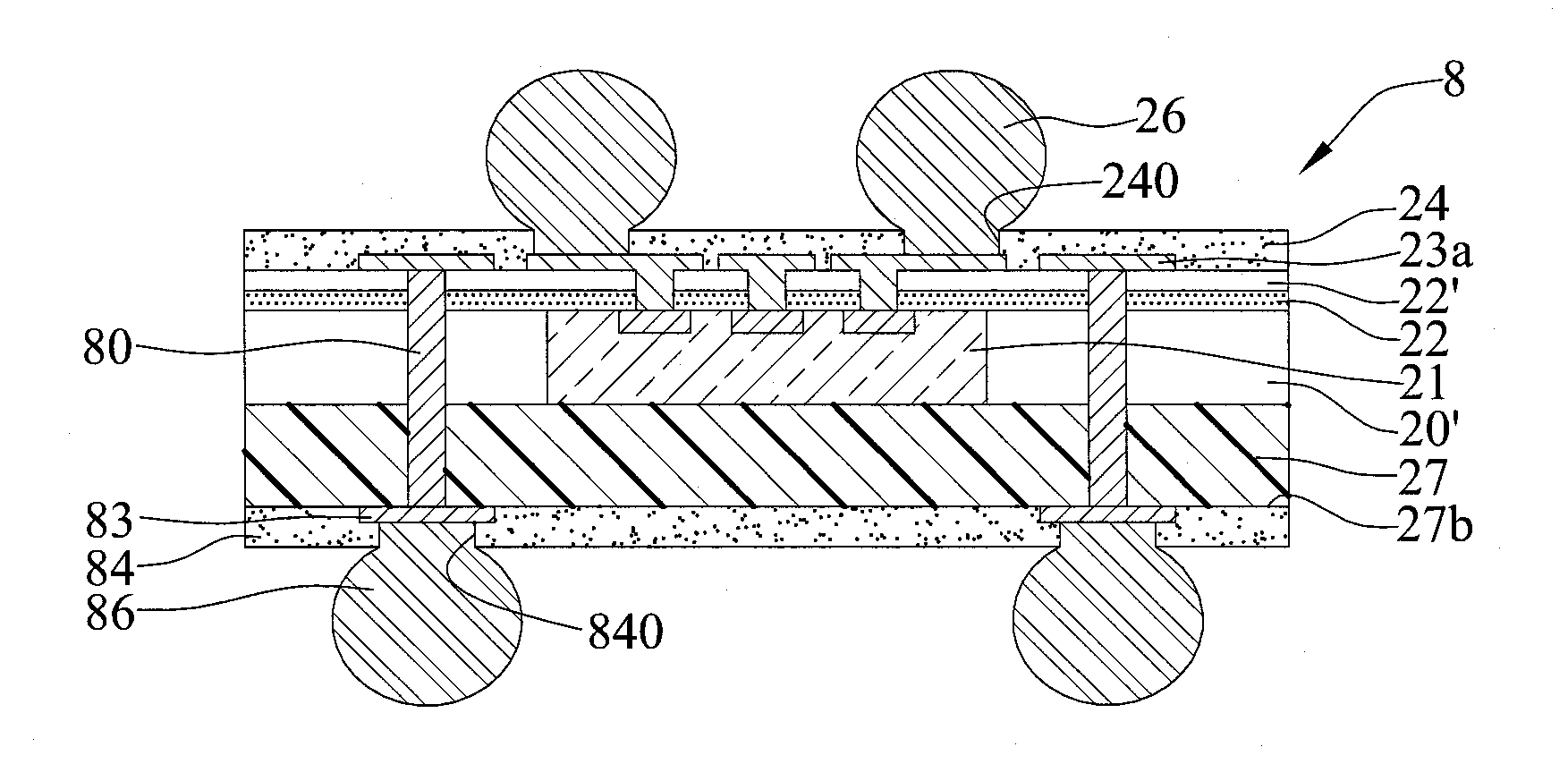
[0037]Referring to FIG. 3, the second embodiment differs from the first embodiment only in that a substrate 30 is further disposed in the second embodiment.

[0038]In the package 3, a substrate 30 is disposed on the second surface 20b of the encapsulating layer 20 and the inactive surface 21b of the chip 21.

[0039]The substrate 30 has a top surface 30a and a bottom surface 30b. Circuits 31 and 32 connected to each other are formed on the top surface 30a and the bottom surface 30b, respectively. The top surface 30a is attached to the second surface 20b of the encapsulating layer 20 and the inactive surface 21b of the chip 21. The circuit 31 on the top surface 30a is embedded into the encapsulating layer 20. A plurality of conductive elements 33 are disposed on the circuit 31 on the top surface 30a and electrically connected to the conductive blind vias 230′ of the circuit layer 23.

[0040]In the second embodiment, the circuits 31 and 32 are electrically connected to each other by conducti...

third embodiment

[0044]Referring to FIGS. 4 and 4′ the third embodiment differs from the first embodiment only in that conductive bumps 40 and 40′ are further disposed in the chip-scale package of the third embodiment.

[0045]In the package 4, 4′, conductive bumps 40, 40′ are disposed in the encapsulating layer 20. The conductive bumps 40, 40′ have top ends combined with the buffering dielectric layer 22 and bottom ends exposed from the second surface 20b, 20b′ of the encapsulating layer 20, 20′, to further combine with conductive elements (e.g., metal wire, solder, solder balls) 46. The circuit layer 23 is electrically connected through the conductive blind vias 230′ to the top ends of the conductive bumps 40, 40′.

[0046]In the fourth embodiment, the conductive bumps 40, 40′ are made of copper.

[0047]As shown in FIG. 4, a metal layer 41 is formed on the bottom ends of the conductive bumps 40, for the conductive elements 46 to be coupled therewith.

[0048]The bottom ends of the conductive bumps 40 are exp...


PUM


Abstract

A chip-scale package includes an encapsulating layer, a chip embedded in the encapsulating layer and having an active surface exposed from the encapsulating layer, a buffering dielectric layer formed on the encapsulating layer and the chip, a build-up dielectric layer formed on the buffering dielectric layer, and a circuit layer formed on the build-up dielectric layer and having conductive blind vias penetrating the build-up dielectric layer and being in communication with the openings of the buffering dielectric layer and electrically connected to the chip, wherein the build-up dielectric layer and the buffering dielectric layer are made of different materials. Therefore, delamination does not occur between the buffering dielectric layer and the encapsulating layer, because the buffering dielectric layer is securely bonded to the encapsulating layer and the buffering dielectric layer is evenly distributed on the encapsulating layer.

Description

BACKGROUND OF THE INVENTION[0001]1. Field of the Invention[0002]This invention relates to semiconductor packages, and, more particularly, to a chip-scale package.[0003]2. Description of Related Art[0004]With the advancement of semiconductor technology, a semicondcutor product may be packaged in a variety of types. In order for the semiconductor package to be low-profiled and compact-sized, a chip-scale package (CSP) is brought to the market. The chip-scale package is characterized in that it is equal to or slightly greater than a chip.[0005]As shown in FIG. 1, a chip-scale package 1 of the prior art comprises a hard board 17 such as a silicon carrier board; an encapsulating layer 10 having a first surface 10a and a second surface 10b opposing the first surface 10a, with the second surface 10b installed on the hard board 17, the encapsulating layer 10 being made of soft material, such as Ajinomoto build-up film (ABF) and bismaleimide-triacine (BT); at least one chip 11 embedded into ...

Claims


Application Information

Patent Timeline
Patent Type & Authority Applications(United States)
IPC IPC(8): H01L23/498H01L23/48
CPCH01L23/3114H01L2924/18162H01L2224/04105H01L2224/12105H01L2224/0401H01L2224/73267H01L24/19H01L23/3128H01L2224/32225
Inventor CHANG, CHIANG-CHENGLIU, HUNG-WENHSU, HSI-CHANGLIAO, HSIN-YICHIU, SHIH-KUANG
Owner SILICONWARE PRECISION IND CO LTD
Why Eureka
Try Eureka