Semiconductor Devices and Methods of Fabrication Thereof

a technology of semiconductors and diaphragms, applied in the direction of semiconductor electrostatic transducers, diaphragm construction, coatings, etc., can solve the problem of severe reduction of the mechanical compliance of the microphon

Active Publication Date: 2012-12-20
INFINEON TECH AG
View PDF8 Cites 35 Cited by
  • Summary
  • Abstract
  • Description
  • Claims
  • Application Information

AI Technical Summary

Benefits of technology

[0008]In accordance with an embodiment of the invention, a semiconductor device comprises a membrane layer comprising a plurality of corrugations disposed over a substrate. Each corrugation of the plurality of corrugations have a sidewall and a bottom surface. A radius of curvature of an edge connecting the sidewall and the bottom surface is greater than a thickness of the membrane layer. A radius of curvature of an edge connecting the sidewall and the top surface is greater than the thickness of the membrane layer.
[0009]The foregoing has outlined rather broadly the features of an embodiment of the present invention in order that the detailed description of the invention that follows may be better understood. Additional features and advantages of embodiments of the invention will be described hereinafter, which form the subject of the claims of the invention. It should be appreciated by those skilled in the art that the conception and specific embodiments disclosed may be readily utilized as a basis for modifying or designing other structures or processes for carrying out the same purposes of the present invention. It should also be realized by those skilled in the art that such equivalent constructions do not depart from the spirit and scope of the invention as set forth in the appended claims.

Problems solved by technology

For example, tensile stress severely decreases the mechanical compliance of the microphone.

Method used


Image

  • Semiconductor Devices and Methods of Fabrication Thereof
  • Semiconductor Devices and Methods of Fabrication Thereof
  • Semiconductor Devices and Methods of Fabrication Thereof

Examples


Embodiment Construction

[0025]The making and using of various embodiments are discussed in detail below. It should be appreciated, however, that the present invention provides many applicable inventive concepts that can be embodied in a wide variety of specific contexts. The specific embodiments discussed are merely illustrative of specific ways to make and use the invention, and do not limit the scope of the invention.

[0026]The present invention will be described with respect to various embodiments in a specific context, namely a Micro electro-mechanical systems (MEMS) sensor. The invention may also be applied, however, to other types of semiconductor devices.

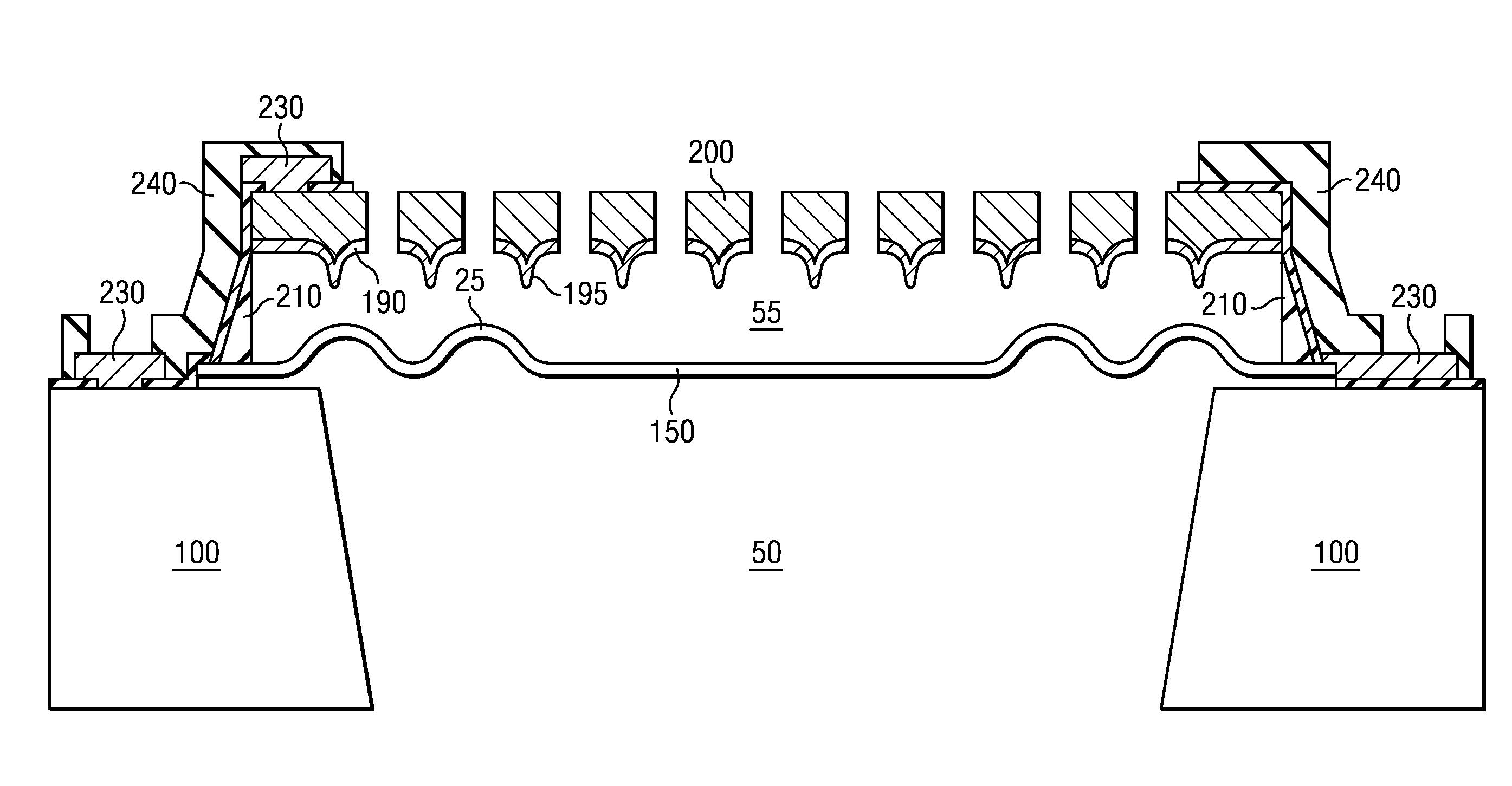
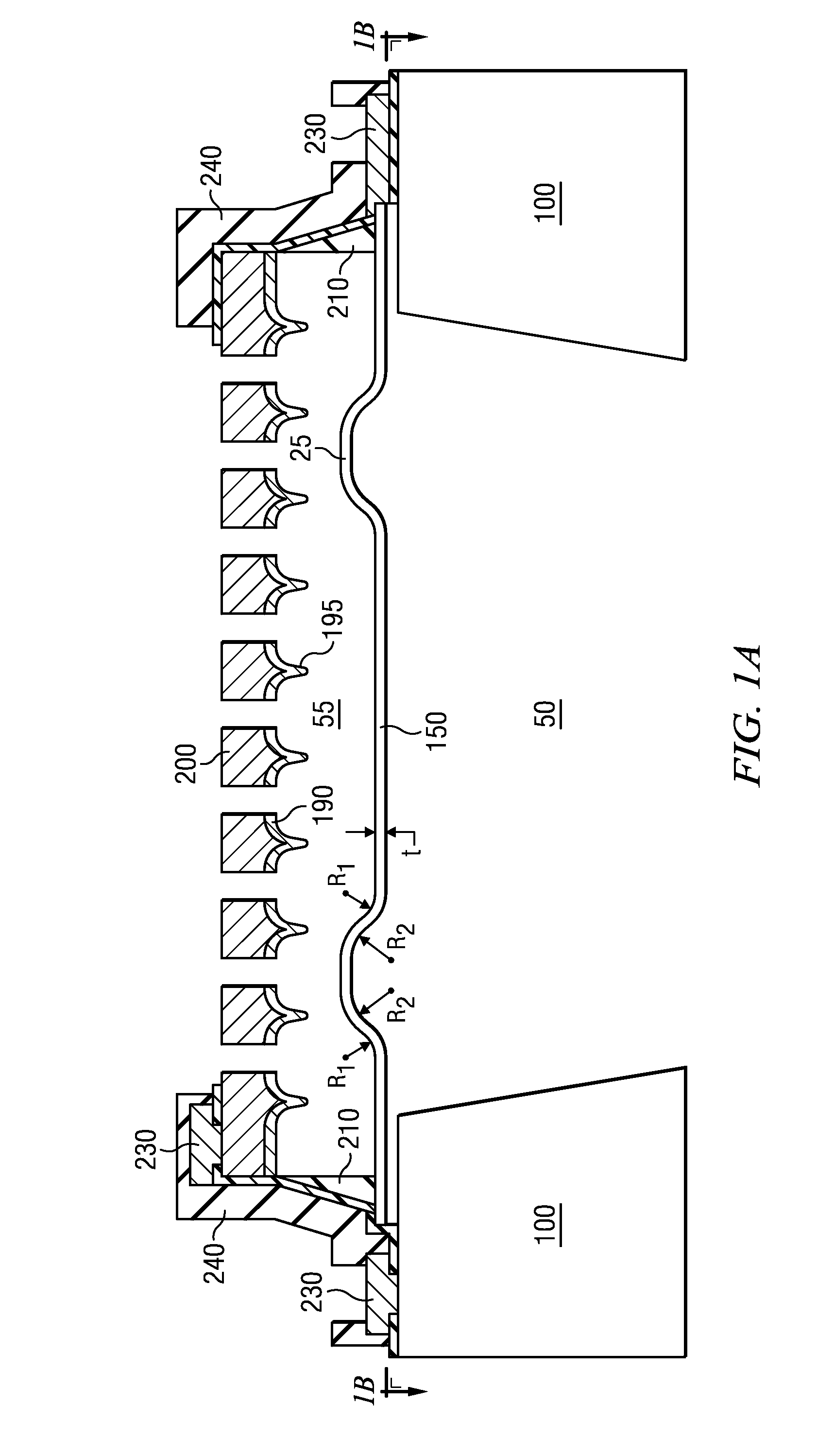
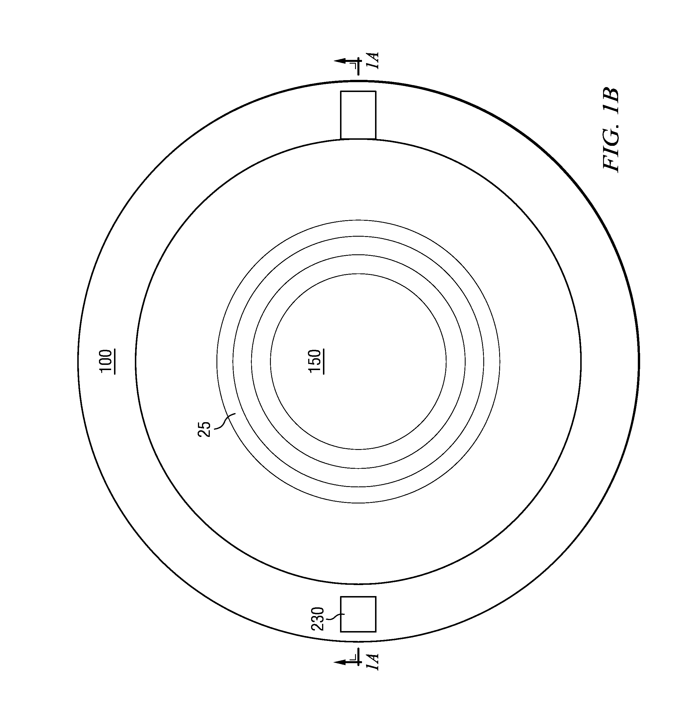
[0027]A structural embodiment of a MEMS sensor will be described using FIG. 1. Further structural embodiments will be described using FIG. 3-5, 11. A method of fabricating the MEMS sensor will be described using FIG. 2. Further methods of fabricating the MEMS sensor will be described usingFIGS. 6-10.

[0028]FIG. 1, which includes FIGS. 1A and 1B, illus...


PUM

PropertyMeasurementUnit
stressaaaaaaaaaa
widthaaaaaaaaaa
depthaaaaaaaaaa

Abstract

In one embodiment, a method of manufacturing a semiconductor device includes oxidizing a substrate to form local oxide regions that extend above a top surface of the substrate. A membrane layer is formed over the local oxide regions and the top surface of the substrate. A portion of the substrate under the membrane layer is removed. The local oxide regions under the membrane layer is removed.

Description

TECHNICAL FIELD[0001]The present invention relates generally to micro-electromechanical systems devices, and more particularly to semiconductor devices and methods of fabrications thereof.BACKGROUND[0002]Small electromechanical components can be manufactured using micro-electromechanical systems (MEMS) technology using microelectronics manufacturing processes. MEMS devices include thin membranes and beams, which function as mechanical and / or electrical components.[0003]Silicon microphone are a type of MEMS device in which the MEMS structure or a membrane actuates with acoustic signals. However, the sensitivity of the membrane, and therefore, the MEMS device varies with stress in the membrane. For example, tensile stress severely decreases the mechanical compliance of the microphone.[0004]Stress may be residual, which is formed during the fabrication, or may build up during operation. Therefore, MEMS devices and methods which minimize film stress are needed.SUMMARY OF THE INVENTION[0...

Claims


Application Information

Patent Timeline
Patent Type & Authority Applications(United States)
IPC IPC(8): H01L29/84H01L21/20
CPCH04R19/005B81B3/0072H01L29/84H04R19/04B81B3/001B81B2201/0257B81C1/00666B81C1/00158B81C1/00182H04R7/14H04R31/003
Inventor DEHE, ALFONSBARZEN, STEFANFRIZA, WOLFGANGKLEIN, WOLFGANG
Owner INFINEON TECH AG
Why Eureka
Try Eureka