System and methods for generating unclonable security keys in integrated circuits

a security key and integrated circuit technology, applied in the field of electrical circuit protection, can solve the problems of difficult cloning, misappropriation or compromise of security keys, complicated design of puf circuits, and less attractive security applications, and achieve the effects of reducing the vulnerability of embedded security keys stored on ics, reducing the risk of cloning, misappropriation or compromis

Active Publication Date: 2012-12-20
STC UNM
View PDF8 Cites 34 Cited by
  • Summary
  • Abstract
  • Description
  • Claims
  • Application Information

AI Technical Summary

Benefits of technology

[0008]According to the present invention, the vulnerability of an embedded security key stored on an IC is mitigated by deriving the security key from the physical characteristics of the IC. A physical unclonable function (“PUF”) circuit generates a silicon-variation-based security key. The PUF circuit includes a specialized electrical hardware circuit that is sensitive to process variations. The PUF further includes a mechanism to retrieve a unique set of responses from a variety of different challenges. A security key derived from a PUF circuit has properties such as volatility and non-replicability, which make it extremely difficult to clone, misappropriate or compromise the security key.

Problems solved by technology

A security key derived from a PUF circuit has properties such as volatility and non-replicability, which make it extremely difficult to clone, misappropriate or compromise the security key.
However, calibration of the environmental conditions may complicate the design of the PUF circuit and make them less attractive for security applications.
Since the power grid is an existing and distributed resource in every design of an IC, the space required by a power grid-derived PUF is limited to the area available for the added challenge / response circuitry.
Moreover, the distributed nature of the power grid makes it more prone to larger random and systematic process variation effects.

Method used


Image

  • System and methods for generating unclonable security keys in integrated circuits
  • System and methods for generating unclonable security keys in integrated circuits
  • System and methods for generating unclonable security keys in integrated circuits

Examples


embodiment 90

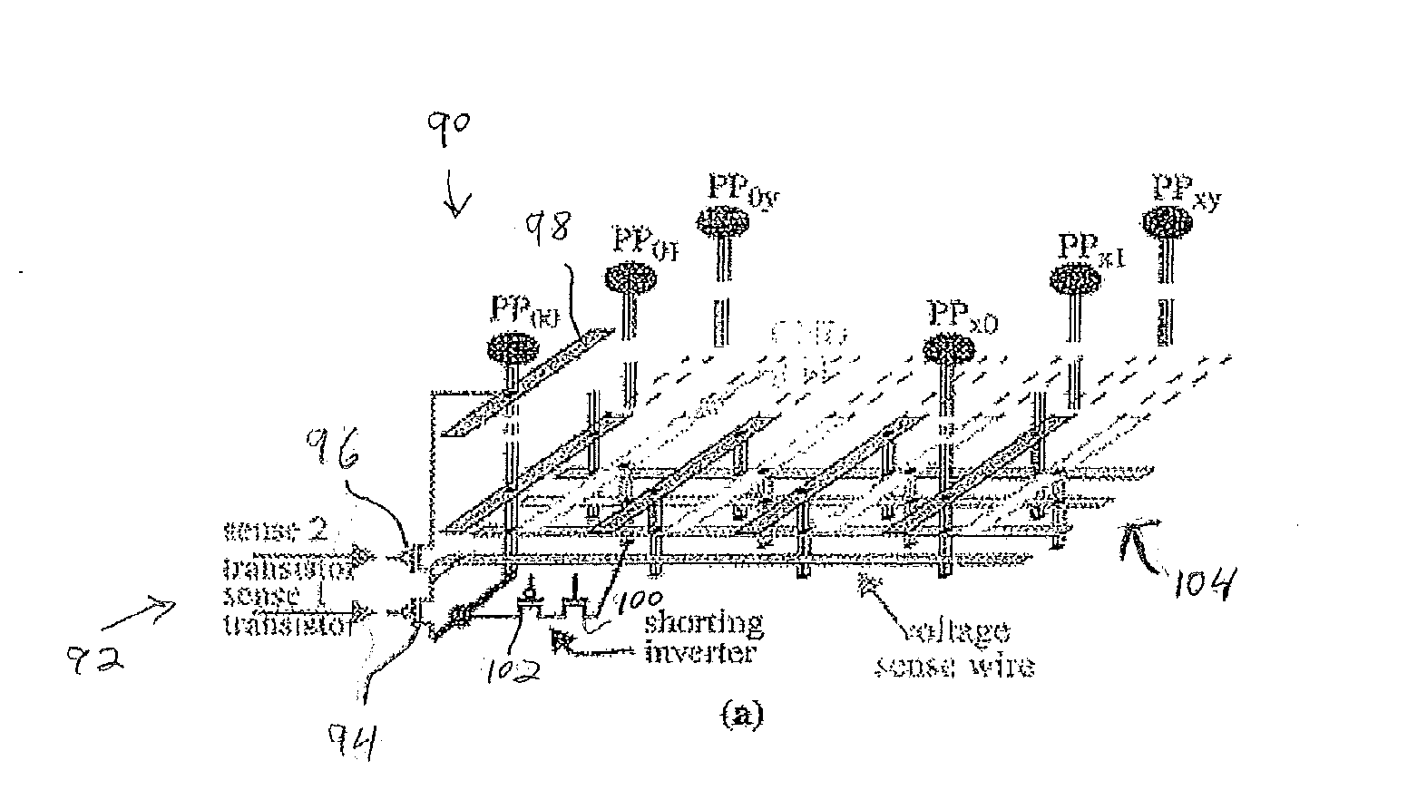
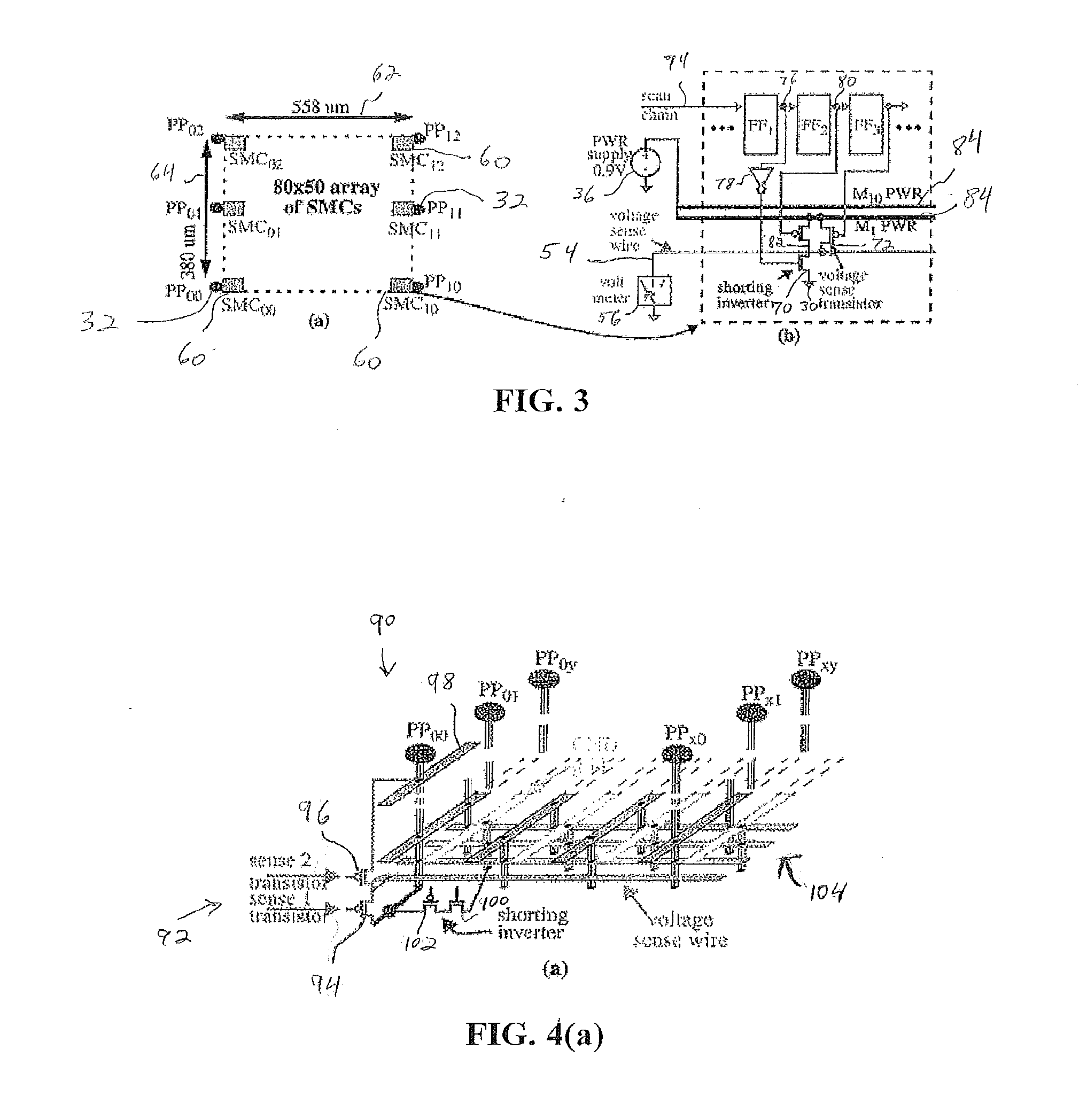
[0042]FIG. 4(b) further illustrates the embodiment 90 having the modified SMC 92, and has like components of FIG. 3(b) identified with similar references numbers. The SMC 90 includes a shorting inverter having a lower transistor 100 that has a drain connected to the ground grid 30, a first voltage sense transistor 94 that has a drain connected to the voltage sense wire 54, and a set of three scan flip-flops FF1, FF2, and FF3. The volt meter 56 is connected to the voltage sense wire 54 and measures the voltage at this node of the SMC circuit 90. The flip-flop FF1 receives a scan chain input 74. The flip-flop FF1 further provides an output 76 to the flip-flop FF2 and an inverter 78. Output from the inverter 78 is provided to the gate of the lower transistor 100 of the shorting inverter. Output from the flip-flop FF1 is also provided via line 106 to the gate of the upper transistor 102 of the shorting inverter. The flip-flop FF2 has an output 80 provided to flip-flop FF3 and also a gat...

embodiment 110

[0045]In another embodiment 110 of the present invention shown in FIG. 5, an increase in the number of stimulus / response pairs is provided, which allows the stimulus to be applied from more than one SMC. In this embodiment 110, multiple shorting inverters are enabled simultaneously at different locations and the voltage drops are measured using different combinations of transistor pairs each connected to one of a first voltage sense wire 112 or a second voltage sense wire 114. The present application refers to these scenarios as “multiple-on” scenarios and the former embodiments 60 and 90 as “single-on” scenarios. Since the power grid is a linear system, superposition applies. Therefore, to make the IC more resilient to attack, where an attacker systematically deduces the voltage drops that would occur under a multiple-on scenario by measuring the voltage drops under all single-on scenarios, the present embodiment can include an obfuscation of the scan chain control bits. Under obfu...

embodiment 130

[0058]Another embodiment 130 of the present invention may provide an increase in the number of single-on scenarios, as shown in FIG. 10. The embodiment 130 can include additional voltage sense transistors 132 that connect to each of the metal layers, e.g., M1 through M10, in a vertical fashion. This allows 10 voltage drops and equivalent resistances based on the number of metal layers to be measured from each SMC. Flip-flops FF2 through FF5 drive the inputs from a respective flip-flop and provide outputs 134-140, respectively, to a 4-to-16 inverting decoder 142 which functions to produce a single low logic ‘0’ on one of the voltage sense transistors when driven with a specific bit pattern. The inverting decoder 142 can be designed such that an input bit pattern of all high logic ‘1’s disables all voltage sense transistors.


PUM

PropertyMeasurementUnit
electrical currentaaaaaaaaaa
widthaaaaaaaaaa
widthaaaaaaaaaa

Abstract

A system and methods that generates a physical unclonable function (“PUF”) security key for an integrated circuit (“IC”) through use of equivalent resistance variations in the power distribution system (“PDS”) to mitigate the vulnerability of security keys to threats including cloning, misappropriation and unauthorized use.

Description

[0001]This application claims the benefit of U.S. Provisional Patent Application No. 61 / 335,939 filed Jan. 12, 2010.FIELD OF THE INVENTION[0002]The present invention relates generally to protection of electrical circuitry used in hardware components, and more specifically, to a system and methods that generates a physical unclonable function (“PUF”) security key for an integrated circuit (“IC”).BACKGROUND OF THE INVENTION[0003]An integrated circuit (“IC”), also known as a chip or a microchip, is a miniaturized electronic circuit used in electronic equipment such as computer, telephone, and digital applications. An IC is typically formed of semiconductor devices, such as silicon and germanium, as well as passive components such as capacitors, resistors, and diodes. Usually, an IC is manufactured on a thin substrate of semiconductor material. In recent years, cost in manufacturing of ICs, per transistor, has decreased. However, while lower cost increases the availability of manufactur...

Claims


Application Information

Patent Timeline
Patent Type & Authority Applications(United States)
IPC IPC(8): H03K19/00H05K3/00G06F21/73
CPCY10T29/49124G06F21/73H04L9/0866Y04S40/24H04L9/0861G09C1/00Y04S40/20
Inventor PLUSQUELLIC, JAMESACHARYYA, DHRUVA J.HELINSKI, RYAN L.
Owner STC UNM
Why Eureka
Try Eureka