Transistor having aluminum metal gate and method of making the same

Inactive Publication Date: 2012-12-27
UNITED MICROELECTRONICS CORP
View PDF1 Cites 18 Cited by
  • Summary
  • Abstract
  • Description
  • Claims
  • Application Information

AI Technical Summary

Benefits of technology

[0006]An objective of the present invention is to provide a transistor having a metal gate and a method for making the same to improve the reliability of transistor performance.
[0009]The present invention utilizes a two-step process for forming the aluminum metal layer of the metal gate, and the two-step process includes the pre-deposition step for the formation of the first aluminum metal layer and the deposition step for the formation of the second aluminum metal layer. An average process temperature of the pre-deposition step is substantially smaller than an average process temperature of the deposition step; additionally, the fluid such as argon (Ar) air is not introduced at the backside of the substrate for heat transfer in the pre-deposition step. The two-step aluminum deposition process decreases the number of pin-hole defects and narrows the grain size distribution of the aluminum metal layer to facilitate the reliability of transistor performance.

Problems solved by technology

With a trend towards scaling down the size of metal-oxide-semiconductors (MOS), the thickness of a gate dielectric layer must be reduced; however, if the gate dielectric layer is insufficient for sustaining a breakdown voltage, the phenomenon of serious leakage current will occur.
Additionally, boron penetration from the polysilicon gate results in a deterioration of the device performance.
Accordingly, how to fabricate an aluminum metal gate having better quality to improve the reliability of transistor performance is still an important issue in the field.

Method used


Image

  • Transistor having aluminum metal gate and method of making the same
  • Transistor having aluminum metal gate and method of making the same
  • Transistor having aluminum metal gate and method of making the same

Examples


Embodiment Construction

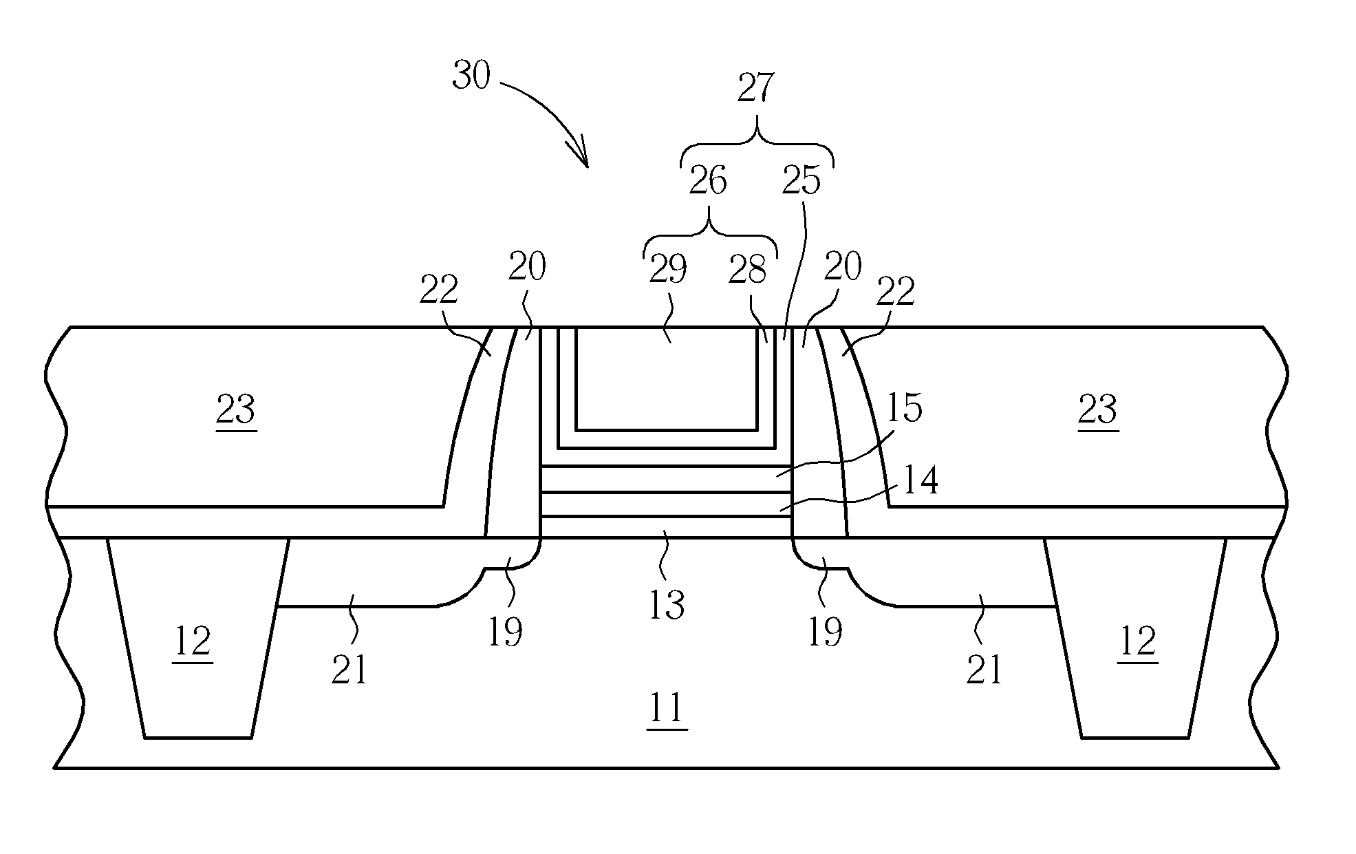
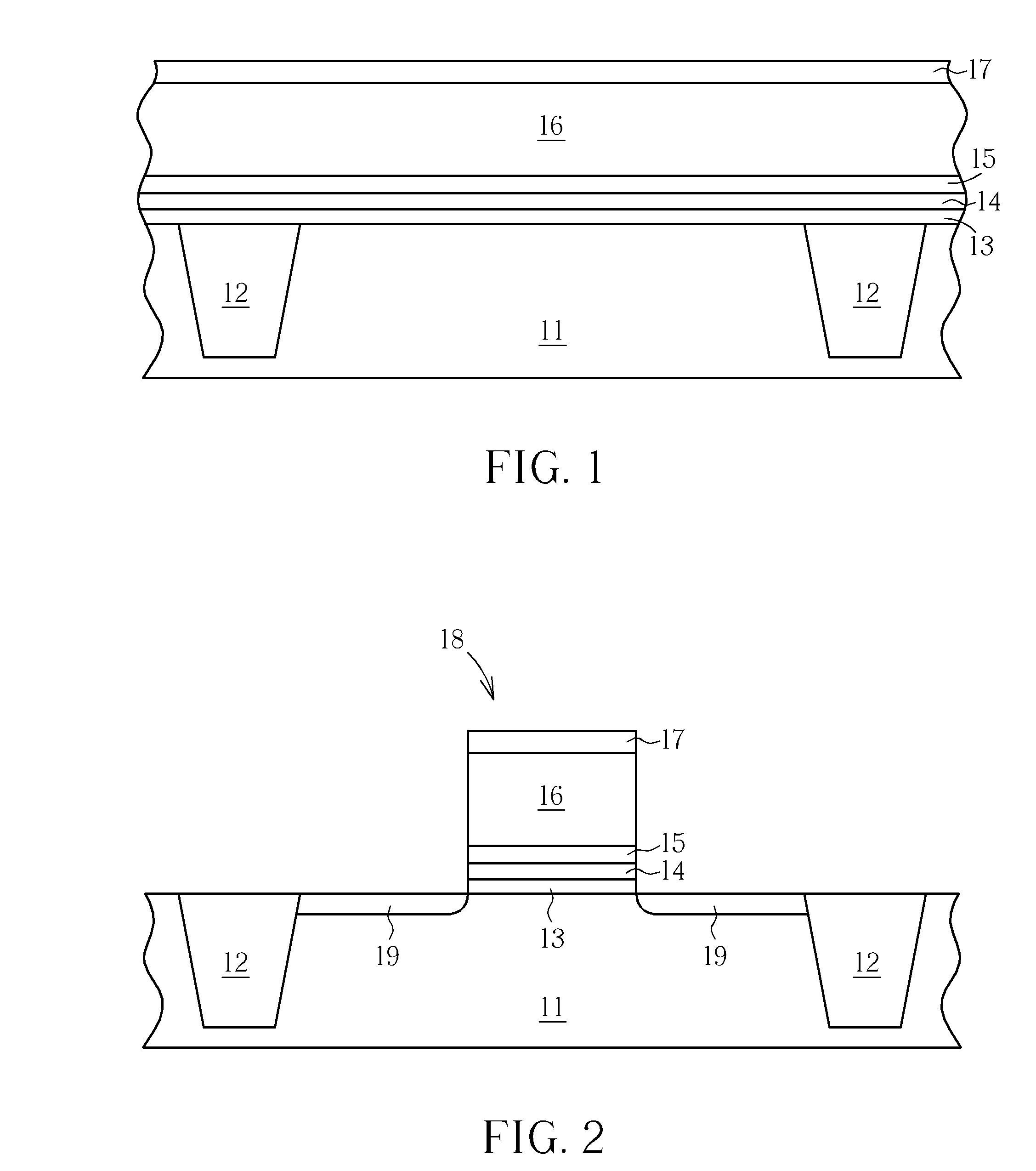
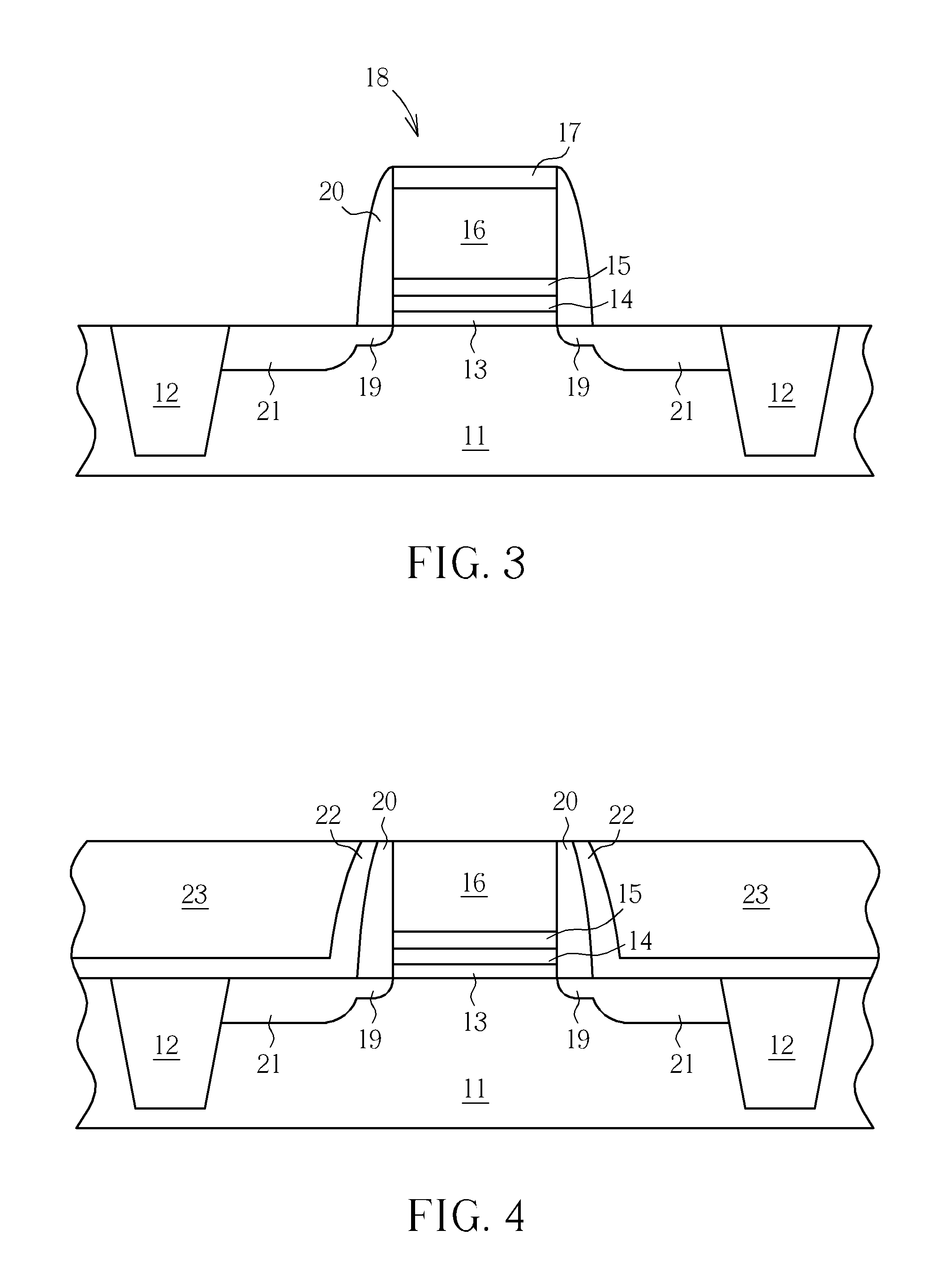
[0013]To provide a better understanding of the present invention, preferred exemplary embodiments will be described in detail. The preferred exemplary embodiments of the present invention are illustrated in the accompanying drawings with numbered elements.

[0014]To eliminate the pin-hole defects caused by the wide grain size distribution of an aluminum metal layer in the physical vapor deposition (PVD) process, the present invention provides a two-step process for forming the aluminum metal layer having a narrower grain size distribution. Please refer to Table. 1. Table. 1 illustrates the gate-fill process steps of the first exemplary embodiment and the second exemplary embodiment. As shown in Table. 1, the process steps of the first exemplary embodiment include: pre-heating, aluminum metal deposition and post-dep reflow. Furthermore, a comparison between the process steps of the first exemplary embodiment and the process steps of the second exemplary embodiment shows that the “pre-h...


PUM


Abstract

A transistor having an aluminum metal gate includes a substrate, a high-k gate dielectric layer, an aluminum metal gate and a source / drain region. The high-k gate dielectric layer is disposed on the substrate. The aluminum metal gate includes a work function tuning layer and an aluminum metal layer disposed orderly on the high-k gate dielectric layer, where the aluminum metal layer comprises a first aluminum metal layer and a second aluminum metal layer. Furthermore, the source / drain region is disposed in the substrate at each of two sides of the aluminum metal gate.

Description

BACKGROUND OF THE INVENTION[0001]1. Field of the Invention[0002]The present invention relates to a transistor having a metal gate and a method for making the same, and more particularly, to a transistor having a metal gate made of an aluminum metal layer with narrower grain size distribution and a method for making the same.[0003]2. Description of the Prior Art[0004]With a trend towards scaling down the size of metal-oxide-semiconductors (MOS), the thickness of a gate dielectric layer must be reduced; however, if the gate dielectric layer is insufficient for sustaining a breakdown voltage, the phenomenon of serious leakage current will occur. Additionally, boron penetration from the polysilicon gate results in a deterioration of the device performance. Therefore, the semiconductor industry tends to use metal gates and high-K (high dielectric constant) materials to replace the conventional polysilicon gate and silicon oxide gate dielectric layer.[0005]For facilitating the high-K mate...

Claims


Application Information

Patent Timeline
IPC IPC(8): H01L21/336H01L29/78
CPCH01L29/4966H01L29/513H01L29/7833H01L29/66545H01L29/6659H01L29/517
Inventor HUANG, HSIN-FUHSU, CHI-MAOTSAI, MIN-CHUANLIN, CHIN-FULIN, CHUN-HSIEN
Owner UNITED MICROELECTRONICS CORP
Why Eureka
Try Eureka