Power amplifier

a power amplifier and amplifier technology, applied in the field of power amplifiers, can solve the problems of large loss due to parasitic resistance of inductors, capacitors, switches, etc., and achieve the effect of reducing loss and being less sensitive to the variation of elements or frequency characteristics

Active Publication Date: 2012-12-27
MURATA MFG CO LTD
View PDF3 Cites 2 Cited by
  • Summary
  • Abstract
  • Description
  • Claims
  • Application Information

AI Technical Summary

Benefits of technology

[0006]In view of the above-described problems, an object of the present invention is to provide a power amplifier which can reduce loss and has less sensitive to the variation of elements or frequency characteristics.
[0008]The present invention makes it possible to reduce loss and has less sensitive to the variation of elements or frequency characteristics.

Problems solved by technology

Therefore, since much current flows, loss due to the parasitic resistances of inductors, capacitors, and switches has been large.

Method used


Image

  • Power amplifier
  • Power amplifier
  • Power amplifier

Examples


first embodiment

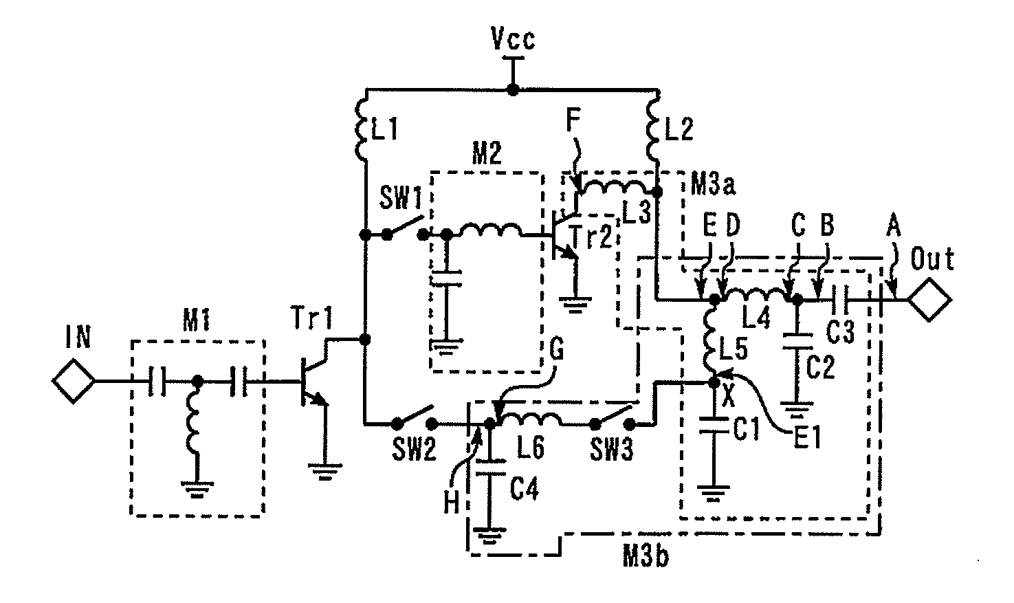
[0028]FIG. 1 is a circuit diagram showing a power amplifier according to a first embodiment of the present invention. The input (base) of an amplifier element Tr1 is connected to the input terminal IN via a matching circuit M1. A switch SW1 and a matching circuit M2 are connected between the output (collector) of the amplifier element Tr1 and the input of the amplifier element Tr2. A matching circuit M3a is connected between the output of an amplifier element Tr2 and an output terminal OUT.

[0029]An end of a switch SW2 is connected to the output of the amplifier element Tr1. The output of the amplifier element Tr1 is connected to the output terminal OUT via the switch SW2 and a matching circuit M3b. To the amplifier elements Tr1 and Tr2, a collector voltage from a power source Vcc is applied via inductors L1 and L2, respectively.

[0030]The output matching circuit has a matching circuit M3a for high outputs, and a matching circuit M3b for low outputs, and both are switched by a switch ...

second embodiment

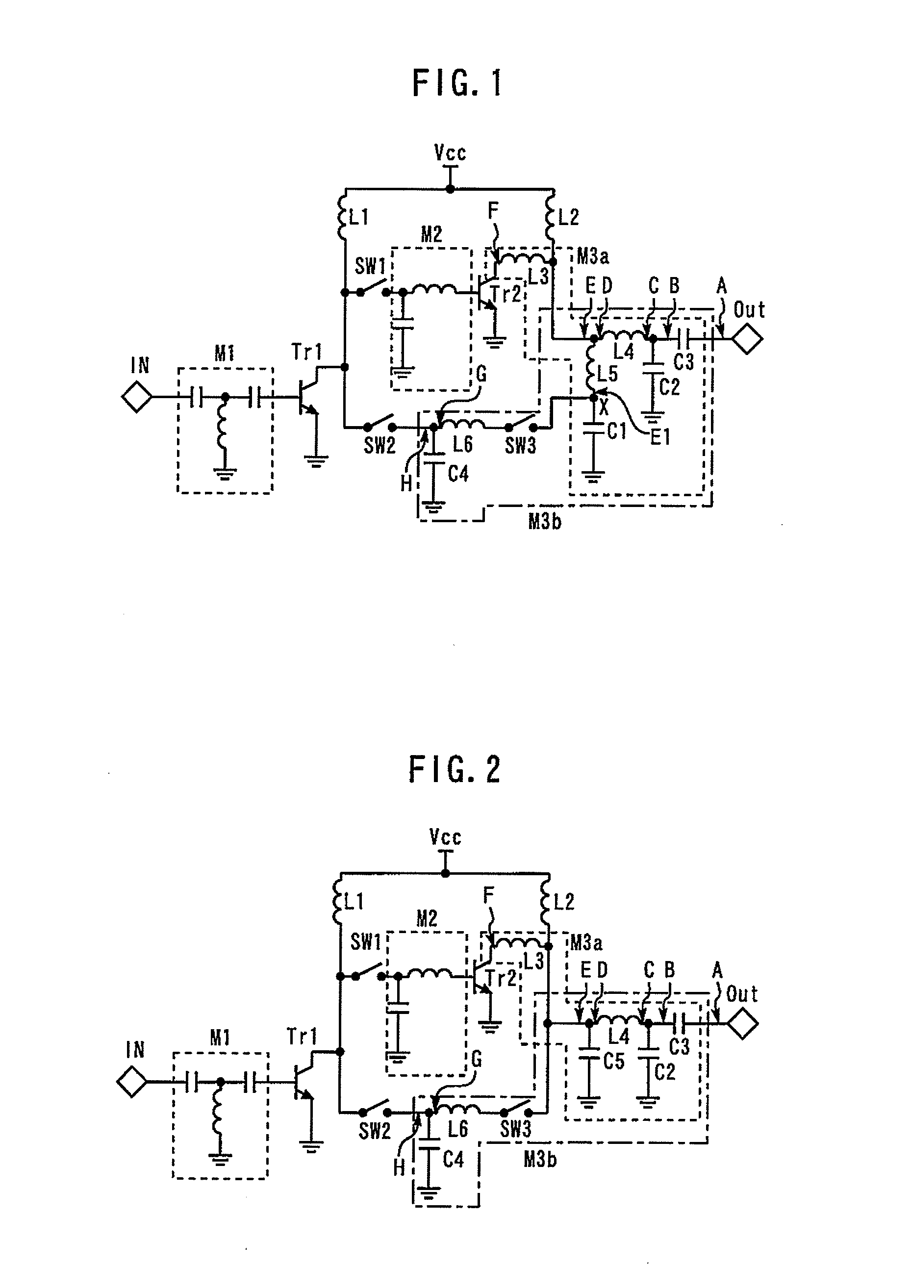
[0039]FIG. 6 is a circuit diagram showing a power amplifier according to a second embodiment of the present invention. The matching circuit M3a for high output is constituted by inductors L3 and L7, and capacitors C2, C3, C5, and C6. The matching circuit M3b for low output is constituted by inductors L6 and L7, and capacitors C2, C3, C4, C5, and C6. Here, the values of L7 and C6 in the second embodiment are set to be seen as the same inductance as the L4 in the comparative example.

jωL4=jωL7+1jωC6[Formula2]

[0040]In the matching circuits M3a and M3b, an inductor L7 and a capacitor C6 is connected in series between the output of the amplifier element Tr2 and the output terminal OUT. The other end of the switch SW2 is connected to the connecting point Y to connect the inductor L7 and the capacitor C6 via the inductor L6 and the switch SW3. The other components are similar to the components of the first embodiment.

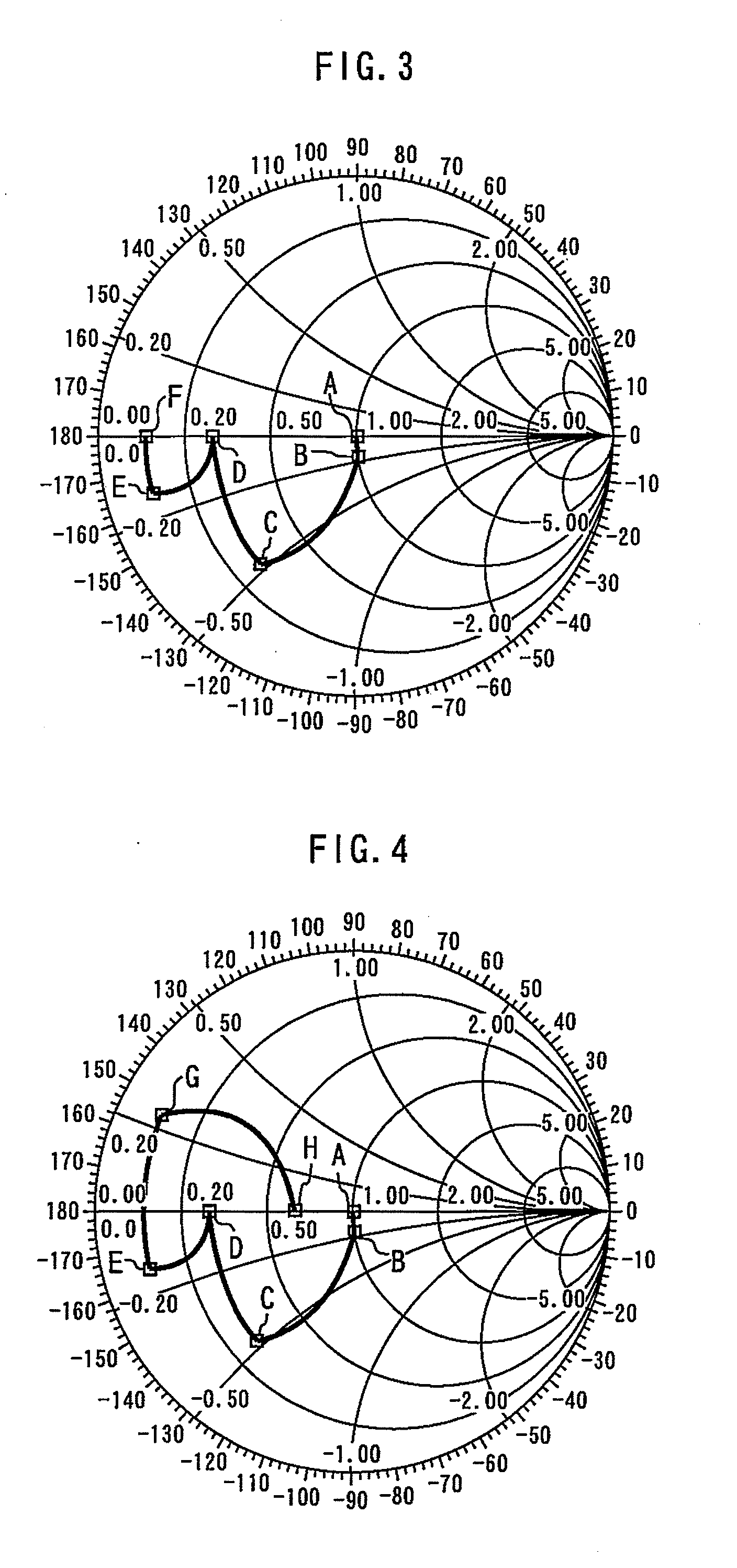
[0041]FIG. 7 is a diagram showing the impedances viewing the output side f...

third embodiment

[0043]FIG. 9 is a circuit diagram showing a power amplifier according to a third embodiment of the present invention. In the third embodiment, the components in the low-gain low-output mode (the third mode) are added to the components of the first embodiment.

[0044]The matching circuit M3a for high output is constituted by the inductors L3, L4, and L5, and the capacitors C1, C2, and C3. The matching circuit M3b for low output is constituted by the inductors L4, L5, L6, L8, and L9, and the capacitors C1, C2, C3, C7, and C8. The matching circuit M3c for low output is constituted by the inductor L9, the capacitor C8, and the switch SW5 in addition to the components of the matching circuit M3b.

[0045]The inductor L7 and the capacitor C8 are connected in series between the other end of the switch SW2 and the grounding point. The inputted signals are amplified by the third amplifier element Tr3. An end of the switch SW4 is connected to the output port of the amplifier element Tr3. The othe...


PUM


Abstract

A power amplifier includes: an input terminal at which an input signal is input; a first amplifier element amplifying the input signal; a second amplifier element amplifying an output signal of the first amplifier element; an output terminal from which an output signal of the second amplifier element is output; a matching circuit connected between an output of the second amplifier element and the output terminal; a first switch connected between an output of the first amplifier element and an input of the second amplifier element; and a second switch having a first end connected to the output of the first amplifier element, and a second end. The matching circuit includes a first inductor and a first capacitor connected in series between the output of the second amplifier element and a grounding point. The second end of the second switch is connected to a connecting point of the first inductor to the first capacitor.

Description

BACKGROUND OF THE INVENTION[0001]1. Field of the Invention[0002]The present invention relates to a power amplifier which is used for a mobile phone etc.[0003]2. Background Art[0004]Since power amplifiers occupy a large weight in the power consumption of mobile phones, making power amplifiers highly efficient is important for reducing power consumption. Therefore, power amplifiers for switching a high-power mode and a low-power mode using a switch have been used (for example, refer to Japanese Patent Application Laid-Open No. 7-336168).SUMMARY OF THE INVENTION[0005]In conventional power amplifiers, the trajectory of impedance viewing the output side from respective points in the output matching circuit for low power has passed through a low-impedance region. Therefore, since much current flows, loss due to the parasitic resistances of inductors, capacitors, and switches has been large. Furthermore, such power amplifiers have been sensitive to the variations of elements, such as induc...

Claims


Application Information

Patent Timeline
Patent Type & Authority Applications(United States)
IPC IPC(8): H03F3/217
CPCH03F1/0277H03F1/565H03F3/191H03F2203/7233H03F3/72H03F2203/21136H03F3/211H03F3/68H03F3/24H04B1/16
Inventor SASAKI, YOSHINOBUYAMAMOTO, KAZUYA
Owner MURATA MFG CO LTD
Why Eureka
Try Eureka