Power module package and method for manufacturing the same
Inactive Publication Date: 2013-01-10
SAMSUNG ELECTRO MECHANICS CO LTD
View PDF4 Cites 8 Cited by
Summary
Abstract
Description
Claims
Application Information
AI Technical Summary
This helps you quickly interpret patents by identifying the three key elements:
Problems solved by technology
Method used
Benefits of technology
Benefits of technology
The present invention is aimed at providing a power module package that is cost-effective and efficient in terms of reducing the area of the heat radiation substrate and minimizing the use of the lead frame for connection to the outside. The technical effects of the invention include reducing product costs and improving overall performance.
Problems solved by technology
Generally, high heat is generated during a power conversion process.
When the generated heat is not effectively removed, performances of the module and the entire system may be deteriorated or damages thereof may be caused.
Therefore, it is difficult to apply the first scheme to applications having a high heat generation amount due to a limitation in heat radiation capability of the lead frame.
In addition, the structure in which a power unit and a control unit are disposed is mainly to perform thermal separation, and has a difficulty in miniaturizing the entire component.
In the case of this scheme, even the control device that does not generate high heat is positioned on an expensive heat radiation substrate, thereby causing an increase in a size of a module itself and increase in a cost of the entire module due to the expensive heat radiation substrate.
In addition, since components having multiple functions are positioned on a single plane, there is a limitation in a degree of freedom in design.
Method used
Image
Click on the blue label to locate the original text in one second.
Reading with bidirectional positioning of images and text.
Examples
first preferred embodiment
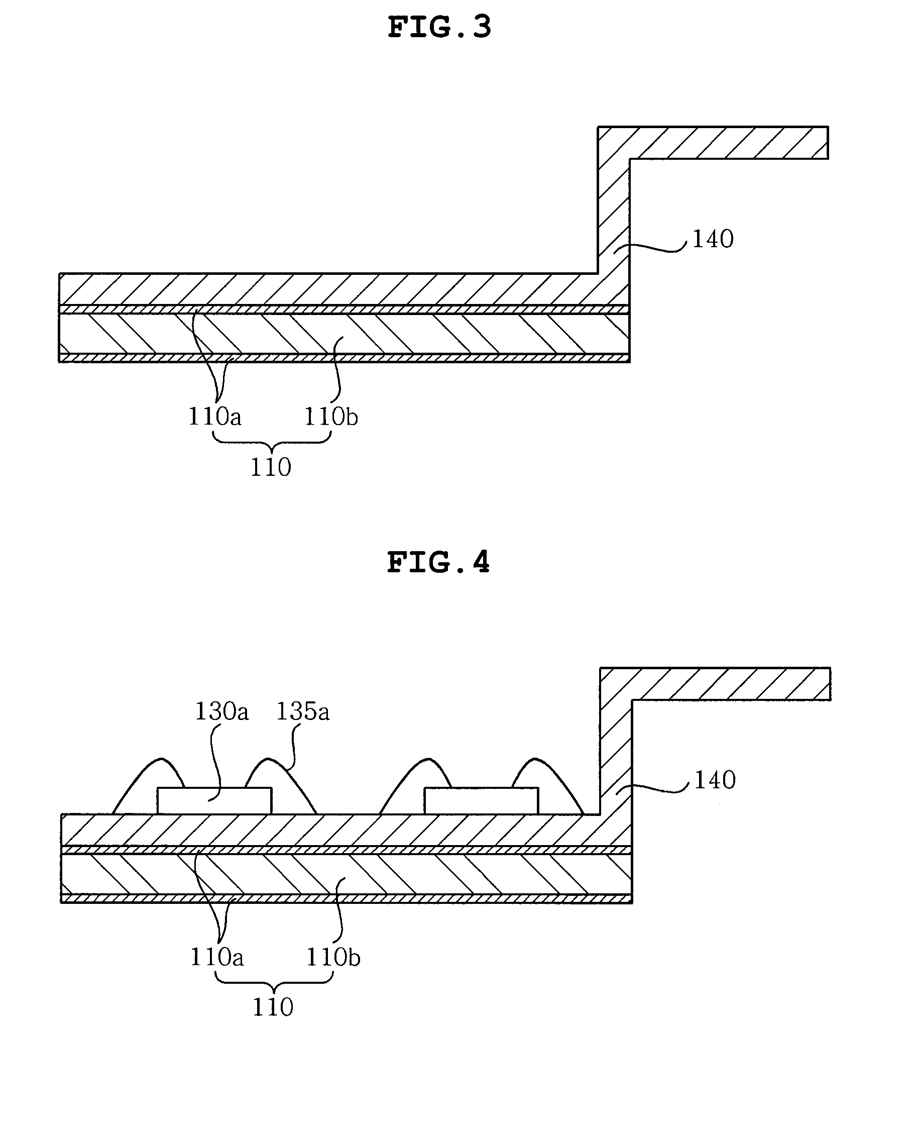
[0081]FIGS. 3 to 8 are process cross-sectional views sequentially showing a method for manufacturing a power module package according to a first preferred embodiment of the present invention.
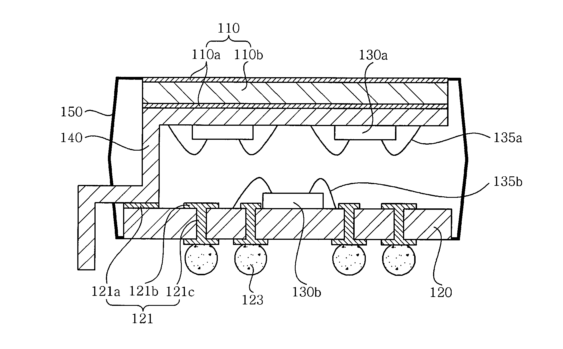
[0082]First, referring to FIG. 3, a first substrate 110 having a lead frame 140 bonded thereto is prepared.
[0083]Here, the first substrate 110 is a substrate having first semiconductor chips 130 mounted thereon. According to the present embodiment, the first substrate 110 may be a metal substrate 110b having anodized layers 110a but is not specifically limited thereto. The first substrate 110 may include, for example, a printed circuit board (PCB), a ceramic substrate, and a directed bonded copper (DBC) substrate.
[0084]As a material of the metal substrate 110b, for example, aluminum (Al) which is a metal material capable of being easily obtained at a relatively low cost and has significantly excellent heat transfer characteristics, or an alloy thereof may be used.
[0114]FIGS. 9 to 14 are process cross-sectional views sequentially showing a method for manufacturing a power module package according to a second preferred embodiment of the present invention.
[0115]In the present embodiment, the same reference numerals will be used to describe the same components as the components described in the first preferred embodiment. In addition, a description of components overlapped with the components described in the first preferred embodiment will be omitted.
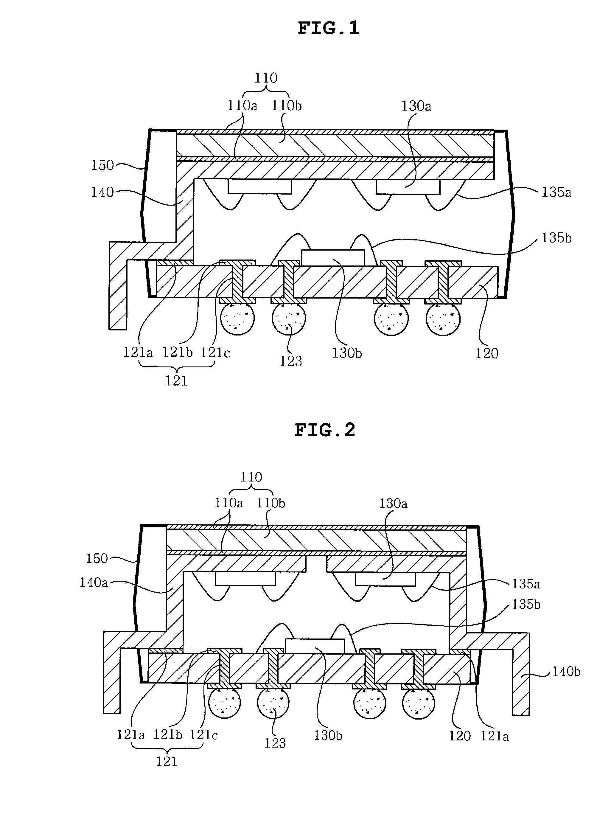
[0116]First, referring to FIG. 9, a first substrate 110 having lead frames 140a and 140b bonded thereto is prepared.
[0117]According to the present embodiment, as shown in FIG. 9, one ends of a pair of lead frames 140a and 140b are bonded to the first substrate 110. Here, the other ends of each of the pair of lead frames 140a and 140b having one ends bonded to the first substrate 110 may have a down-set form but is not specifically limited thereto.
[0118]In addition, although FIG. 9 shows that the pa...
PUM
Abstract
Disclosed herein is a power modulepackage including: a first substrate; a second substrate having a pad for connection to the first substrate formed on one side or both sides of one surface thereof and having external connection terminals for connection to the outside formed on the other surface thereof; and a lead frame having one end bonded to the first substrate and the other end bonded to the pad of the second substrate to thereby vertically connect the first and second substrates to each other.
Description
CROSS REFERENCE TO RELATED APPLICATION[0001]This application claims the benefit of Korean Patent Application No. 10-2011-0066046, filed on Jul. 4, 2011, entitled “Power ModulePackage And Method For Manufacturing The Same”, which is hereby incorporated by reference in its entirety into this application.BACKGROUND OF THE INVENTION[0002]1. Technical Field[0003]The present invention relates to a power modulepackage and a method for manufacturing the same.[0004]2. Description of the Prior Art[0005]In accordance with a global increase in energy usage, the use of a power conversion device such as an inverter in fields such as home appliances, industrial products, or the like has increased in order to effectively use energy and protect environment.[0006]An intelligent power module (IPM) that has been prominent in accordance with the increase in the use of the inverter is a core component performing direct current (DC) rectification and alternate current (AC) conversion in the inverter and...
Claims
Application Information
Patent Timeline
Application Date:The date an application was filed.
Publication Date:The date a patent or application was officially published.
First Publication Date:The earliest publication date of a patent with the same application number.
Issue Date:Publication date of the patent grant document.
PCT Entry Date:The Entry date of PCT National Phase.
Estimated Expiry Date:The statutory expiry date of a patent right according to the Patent Law, and it is the longest term of protection that the patent right can achieve without the termination of the patent right due to other reasons(Term extension factor has been taken into account ).
Invalid Date:Actual expiry date is based on effective date or publication date of legal transaction data of invalid patent.

