Nonvolatile memory element, manufacturing method thereof, nonvolatile memory device, and design support method for nonvolatile memory element

a technology of nonvolatile memory and manufacturing method, which is applied in the direction of bulk negative resistance effect devices, program control, instruments, etc., can solve the problem of limiting the miniaturization of existing flash memories using floating gates, and achieve the reduction of initialization voltage, facilitate formation of conductive paths, and leak current in variable resistance layers

Active Publication Date: 2013-01-10
PANASONIC SEMICON SOLUTIONS CO LTD
View PDF5 Cites 24 Cited by
  • Summary
  • Abstract
  • Description
  • Claims
  • Application Information

AI Technical Summary

Benefits of technology

[0037]According to an implementation of the present invention, the maximum area of the second transition metal oxide in the plane direction is reduced so that the leak current in the variable resistance layer is reduced and the density of current flowing to the first variable resistance layer is increased, which reduces the initialization voltage for initializing the variable resistance element and facilitates formation of a conductive path in the first variable resistance layer, thereby producing an effect that the nonvolatile memory element can be initialized at low voltage.
[0038]Furthermore, with the method of manufacturing the nonvolatile memory element according to an aspect of the present invention, a damaged layer is recovered by nitridation or fluorination of the lateral side of the nonvolatile memory element, and the current density of current possible to flow in the nonvolatile memory element increases, with the result that the initialization voltage for the nonvolatile memory element is reduced.
[0039]Furthermore, as compared to the case of using a transition metal oxide, the use of the transition metal compound allows a further reduction in the volume increase and makes it further possible to reduce the separation between the u...

Problems solved by technology

In response to such a demand, it is said that there is a limit o...

Method used


Image

  • Nonvolatile memory element, manufacturing method thereof, nonvolatile memory device, and design support method for nonvolatile memory element
  • Nonvolatile memory element, manufacturing method thereof, nonvolatile memory device, and design support method for nonvolatile memory element
  • Nonvolatile memory element, manufacturing method thereof, nonvolatile memory device, and design support method for nonvolatile memory element

Examples


first embodiment

[0093]First, a nonvolatile memory element according to the first embodiment of the present invention is described.

[0094][Structure]

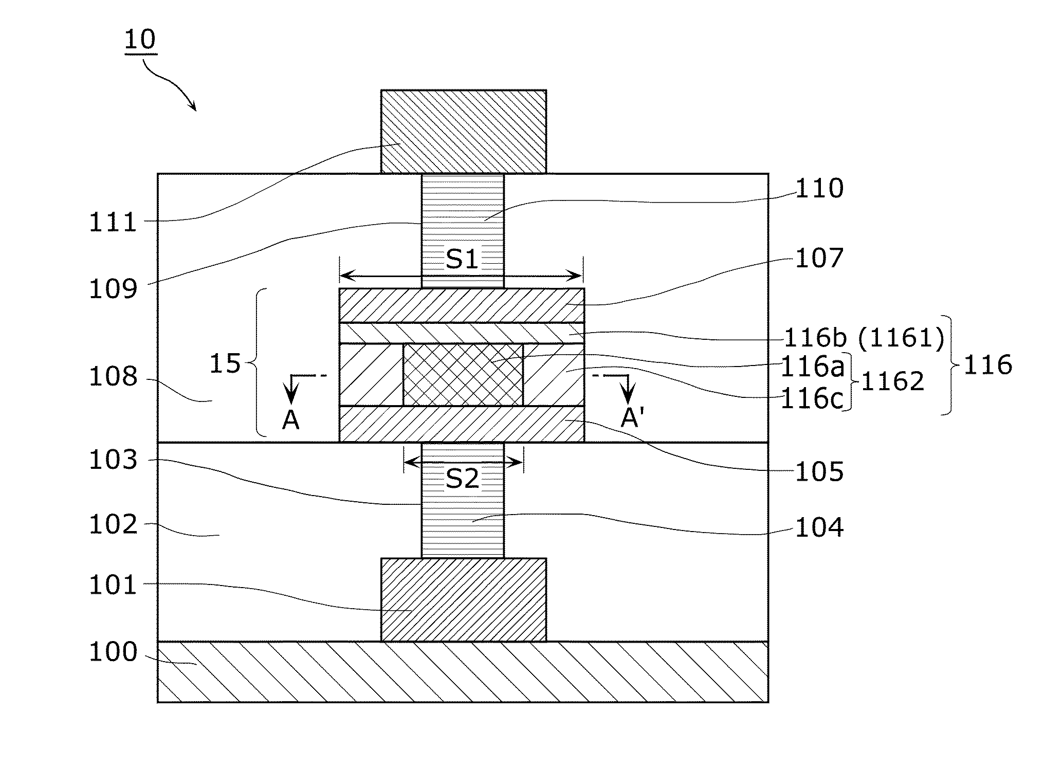
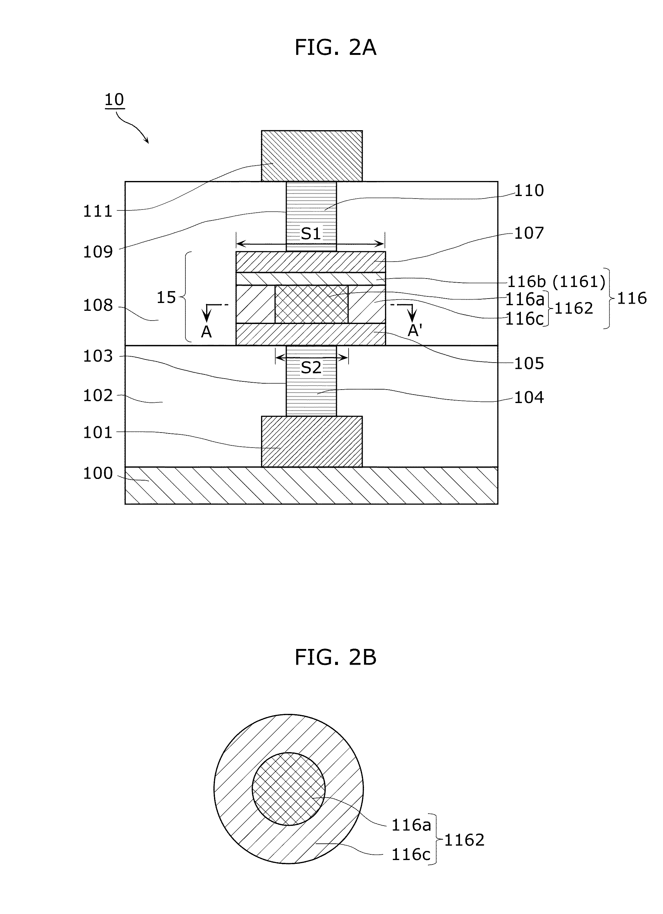
[0095]FIG. 2A is a cross-sectional view of a nonvolatile memory element 10 according to the first embodiment of the present invention. FIG. 2B shows a cross-sectional view taken along A-A′ of FIG. 2A. As shown in FIG. 2A, the nonvolatile memory element 10 according to this embodiment is a variable resistance nonvolatile memory element and includes a substrate 100, a first line 101, a first interlayer insulating layer 102, a first contact plug 104, a variable resistance element 15, a second interlayer insulating layer 108, a second contact plug 110, and a second line 111. In a practical structure of a memory cell using the nonvolatile memory element 10 according to this embodiment, one of the first line 101 and the second line 111 is connected to a switching element (i.e., a diode or a transistor) which is set to be ON when the cell is selected and be OFF...

second embodiment

[0143]Next, a nonvolatile memory element according to the second embodiment of the present invention is described.

[0144][Structure]

[0145]FIG. 14 is a cross-sectional view of a nonvolatile memory element 20 according to the second embodiment of the present invention. FIG. 14B shows a cross-sectional view taken along B-B′ of FIG. 14A and viewed in the direction of the arrows. As shown in FIG. 14A, the nonvolatile memory element 20 according to this second embodiment is a variable resistance nonvolatile memory element and includes the substrate 100 comprising silicon (Si) or the like, the first line 101, the first interlayer insulating layer 102, the first contact plug 104, a variable resistance element 25, the second interlayer insulating layer 108, the second contact plug 110, and the second line 111.

[0146]The variable resistance element 25 includes the lower electrode 105, a variable resistance layer 126, and the upper electrode 107. The variable resistance layer 126 is a layer disp...

third embodiment

[0159]Next, a nonvolatile memory element according to the third embodiment of the present invention is described.

[0160][Structure]

[0161]FIG. 16 is a cross-sectional view of a nonvolatile memory element 30 according to the third embodiment of the present invention. As shown in FIG. 16, the nonvolatile memory element 30 according to this embodiment is a variable resistance nonvolatile memory element and includes the substrate 100 comprising silicon (Si) or the like, the first line 101, the first interlayer insulating layer 102, the first contact plug 104, a variable resistance element 35, the second interlayer insulating layer 108, the second contact plug 110, and the second line 111. The variable resistance element 35 includes the lower electrode 105, a variable resistance layer 136, and the upper electrode 107. The variable resistance layer 136 is a layer disposed between the lower electrode 105 and the upper electrode 107 and has a resistance value that reversibly changes based on ...


PUM


Abstract

A nonvolatile memory element includes a variable resistance layer located between a lower electrode and an upper electrode and having a resistance value that reversibly changes based on electrical signals applied between these electrodes. The variable resistance layer includes at least two layers: a first variable resistance layer including a first transition metal oxide; and a second variable resistance layer including a second transition metal oxide and a transition metal compound. The second transition metal oxide has an oxygen content atomic percentage lower than an oxygen content atomic percentage of the first transition metal oxide, the transition metal compound contains either oxygen and nitrogen or oxygen and fluorine, and the second transition metal oxide and the transition metal compound are in contact with the first variable resistance layer.

Description

TECHNICAL FIELD[0001]The present invention relates to nonvolatile memory elements, methods of manufacturing the same, nonvolatile memory devices, and design support methods for nonvolatile memory elements, and particularly to a variable resistance nonvolatile memory element including a variable resistance layer of which resistance has a value changing by application of electric pulses and is maintained at the changed value, and to a method of manufacturing the variable resistance nonvolatile memory element.BACKGROUND ART[0002]In recent years, along with development of the digital technology, electronic devices such as portable information devices and information home appliances have increasingly higher-level functionalities. There is thus a higher demand on nonvolatile memory elements for an increase in capacity, a reduction in power for writing, an increase in speed for writing / reading, and a longer operating life.[0003]In response to such a demand, it is said that there is a limit...

Claims


Application Information

Patent Timeline
IPC IPC(8): H01L45/00G11C11/00G06F17/50
CPCG11C13/0007G11C2213/32G11C2213/34G11C2213/55H01L27/101H01L27/02H01L27/2427H01L45/1233H01L45/146H01L45/1625H01L45/1641H01L45/1675H01L27/2436H01L45/08H10B63/30H10N70/24H10N70/826H10N70/8833H10N70/026H10N70/041H10N70/063H10B63/24
Inventor HAYAKAWA, YUKIOMIKAWA, TAKUMININOMIYA, TAKEKI
Owner PANASONIC SEMICON SOLUTIONS CO LTD
Why Eureka
Try Eureka