Polariton based all-optical spin device

a technology of all-optical spin and polariton, applied in the field of optical memory and logic gates, can solve the problems of difficult control, fluctuations and losses, and affect the communication between optical stages, and can be difficult to control

Inactive Publication Date: 2013-01-17
ECOLE POLYTECHNIQUE FEDERALE DE LAUSANNE (EPFL)
View PDF1 Cites 1 Cited by
  • Summary
  • Abstract
  • Description
  • Claims
  • Application Information

AI Technical Summary

Problems solved by technology

However the existing solutions using semiconductor heterostructures often rely on the relative phase between the switching pulses (see for instance EP 0809128 and EP 1128204 A1), which is difficult to control, and prevent to write information by sending pulses with arbitrary time delays.
One problem with this approach is that different wavelengths with specific requirements are involved.
As a consequence there is no cascadability, meaning that output of such a gate cannot be used as input for an identical gate, preventing for building arrays.
However the proposal of a RAM device (see Ref 7) relies on the control of the relative phase between the switching pulses, which has previously been shown to be problematic.
However, for most all-optical logic circuits schemes, fluctuations and losses are considered as an important drawback for communication between optical stages.

Method used


Image

  • Polariton based all-optical spin device
  • Polariton based all-optical spin device
  • Polariton based all-optical spin device

Examples


Embodiment Construction

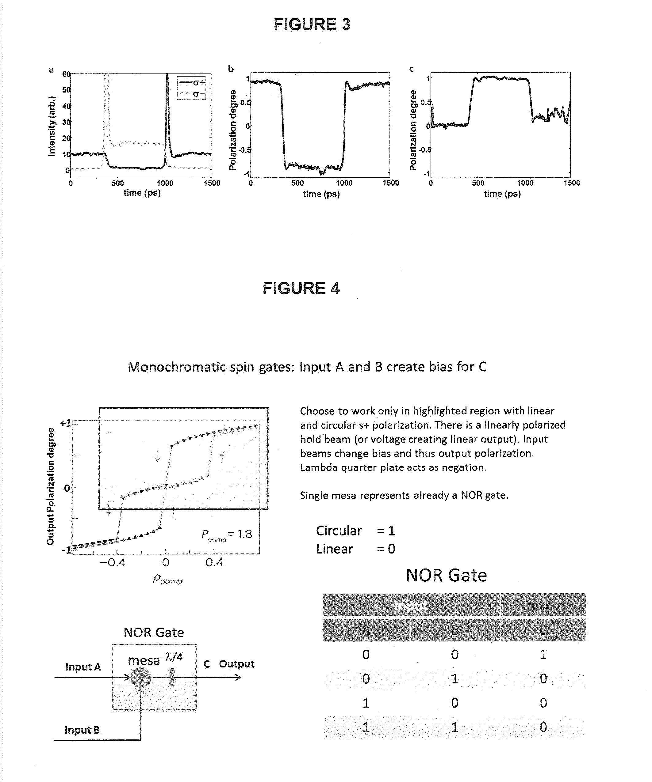
[0036]An elegant way of solving the problems mentioned in the previous sections is to encode logic levels independently from the optical intensity. Optical spinor systems are therefore excellent candidates to develop such devices since the spin polarization can be used for storing information as well as for logic operations.

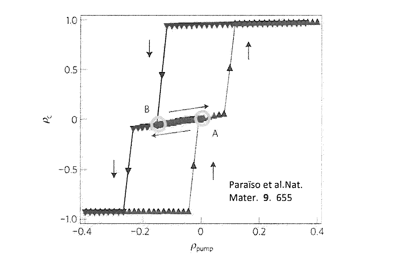
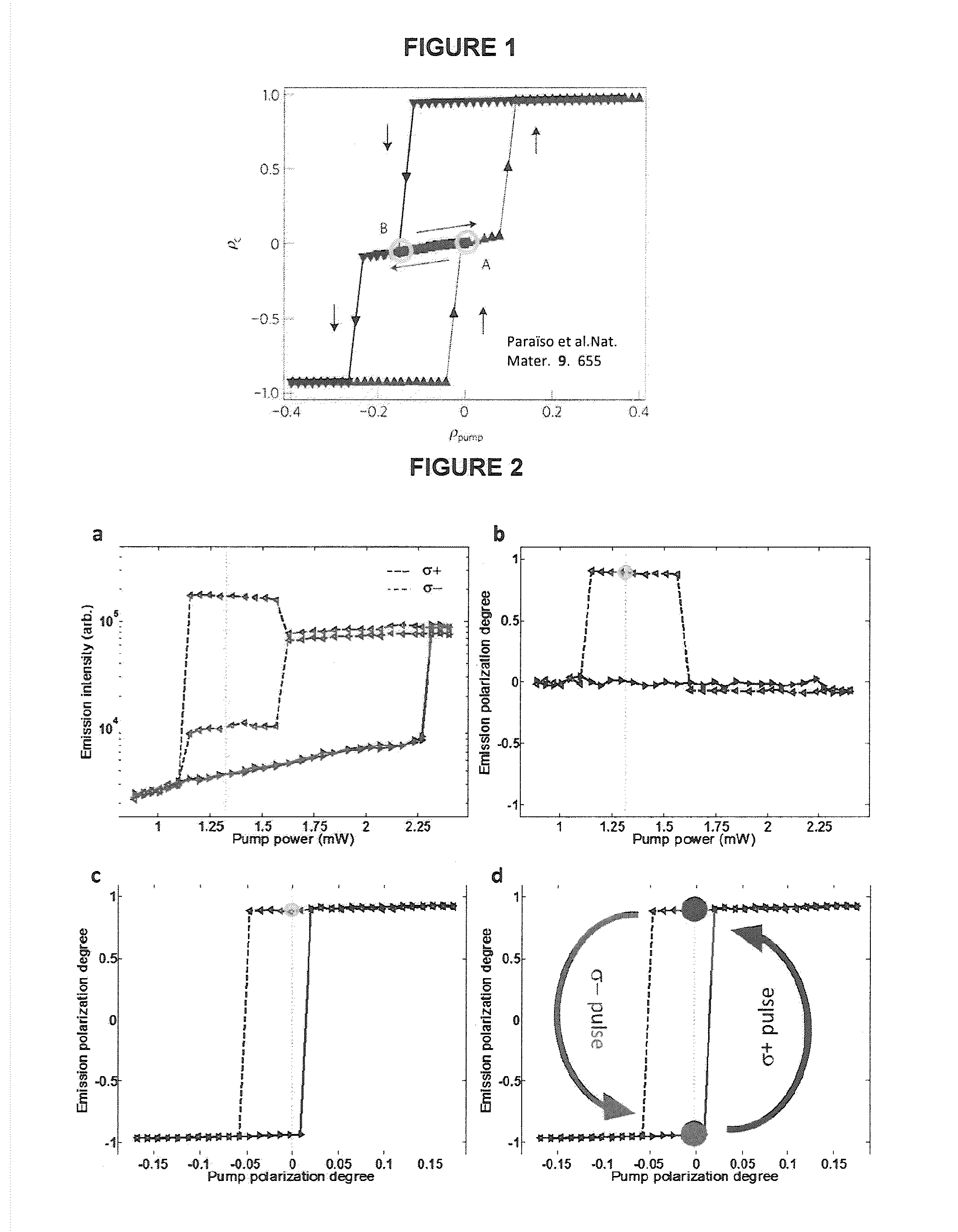
[0037]The invention therefore relates to an all-optical spin device based on spin multistability of trapped microcavity polaritons.

[0038]The device according to the present invention may admit two or more stable spin states for a given single optical excitation condition. The device is preferably driven by a single wavelength continuous wave (cw) excitation laser. This optical cw may be replaced for instance by electrical pumping through resonant tunneling. The switching between the different states can be achieved at constant excitation power by changing the excitation polarization (using a quarter-wave plate). The light emitted by the device has preferably the ...


PUM

PropertyMeasurementUnit
timeaaaaaaaaaa
timeaaaaaaaaaa
Wavelengthaaaaaaaaaa

Abstract

An all-optical spin device is based on spin multistability of trapped microactivity polaritons.

Description

FIELD OF INVENTION[0001]The present invention relates to optical processing and / or, in particular but not exclusively, to optical memories and logic gates.STATE OF THE ART[0002]In the recent years, different groups have developed a variety of optical memories—often referred to as all-optical flip-flops—and of logic gates. A selection of those projects is briefly presented in this chapter.i) Phase Dependent Switches[0003]There are several realizations of optical polarization switches and AOFF working with holding beam and writing pulses. The use of holding beam is important to maintain the polarization state for durations longer than the lifetime of the spin carriers in the device. However the existing solutions using semiconductor heterostructures often rely on the relative phase between the switching pulses (see for instance EP 0809128 and EP 1128204 A1), which is difficult to control, and prevent to write information by sending pulses with arbitrary time delays.ii) Wavelength Depe...

Claims


Application Information

Patent Timeline
Patent Type & Authority Applications(United States)
IPC IPC(8): G02F3/00
CPCG02F3/00G02F2203/16G02F2203/15G02F3/02
Inventor PARA SO, TAOFIQLEGER, YOANCERNA, ROLANDMORIER-GENOUD, FRANCOISDEVEAUD-PLEDRAN, BENO T
Owner ECOLE POLYTECHNIQUE FEDERALE DE LAUSANNE (EPFL)
Why Eureka
Try Eureka