
Impact resistant device comprising an optical layer

Inactive Publication Date: 2013-01-31
SAMSUNG ELECTRONICS CO LTD
View PDF5 Cites 45 Cited by
  • Summary
  • Abstract
  • Description
  • Claims
  • Application Information

AI Technical Summary

Benefits of technology

This patent describes a new way to make solar panels that are stronger without adding extra weight or cost. A special material is used that changes from a solid to a liquid when hit by a force, which helps to absorb the impact and protect the solar cells from damage. This backing structure also allows for a more effective dissipation of energy from the impact, which improves the efficiency of the solar panel.

Problems solved by technology

A problem of current thin display devices is to provide a sufficient impact resistance.
The combination of low weight and high impact resistance cannot be delivered by the current solutions.
Unfortunately, such an impact resistant layer may obscure the view of the optical layer and increase the thickness and / or weight of the thin display device which goes against the aforementioned common desire for a thinner display device.
Disadvantageously, known measures of providing protection to a display device may obscure the view of the optical layer and thereby cause a deterioration of the visual quality of the display.
Also the known measures may provide an undesirable increased thickness and / or weight of the display device.
That is, the stress in the backing material is possibly a complicated function of the strain and the strain rate.
Conventionally, solar panels may be reinforced at the front side, resulting in increased weight, cost and reduced efficiency.

Method used


Image

  • Impact resistant device comprising an optical layer
  • Impact resistant device comprising an optical layer
  • Impact resistant device comprising an optical layer

Examples


Embodiment Construction

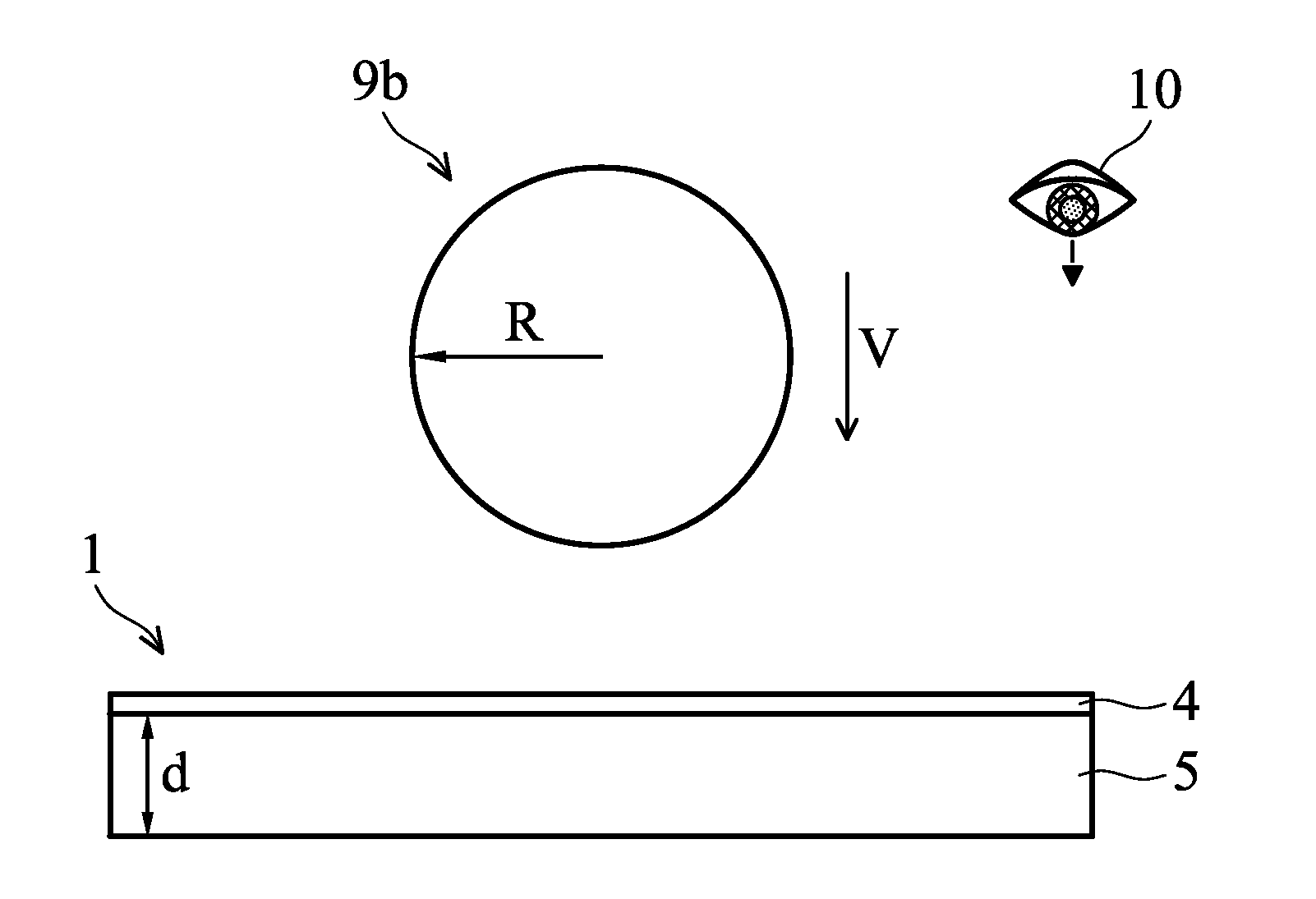
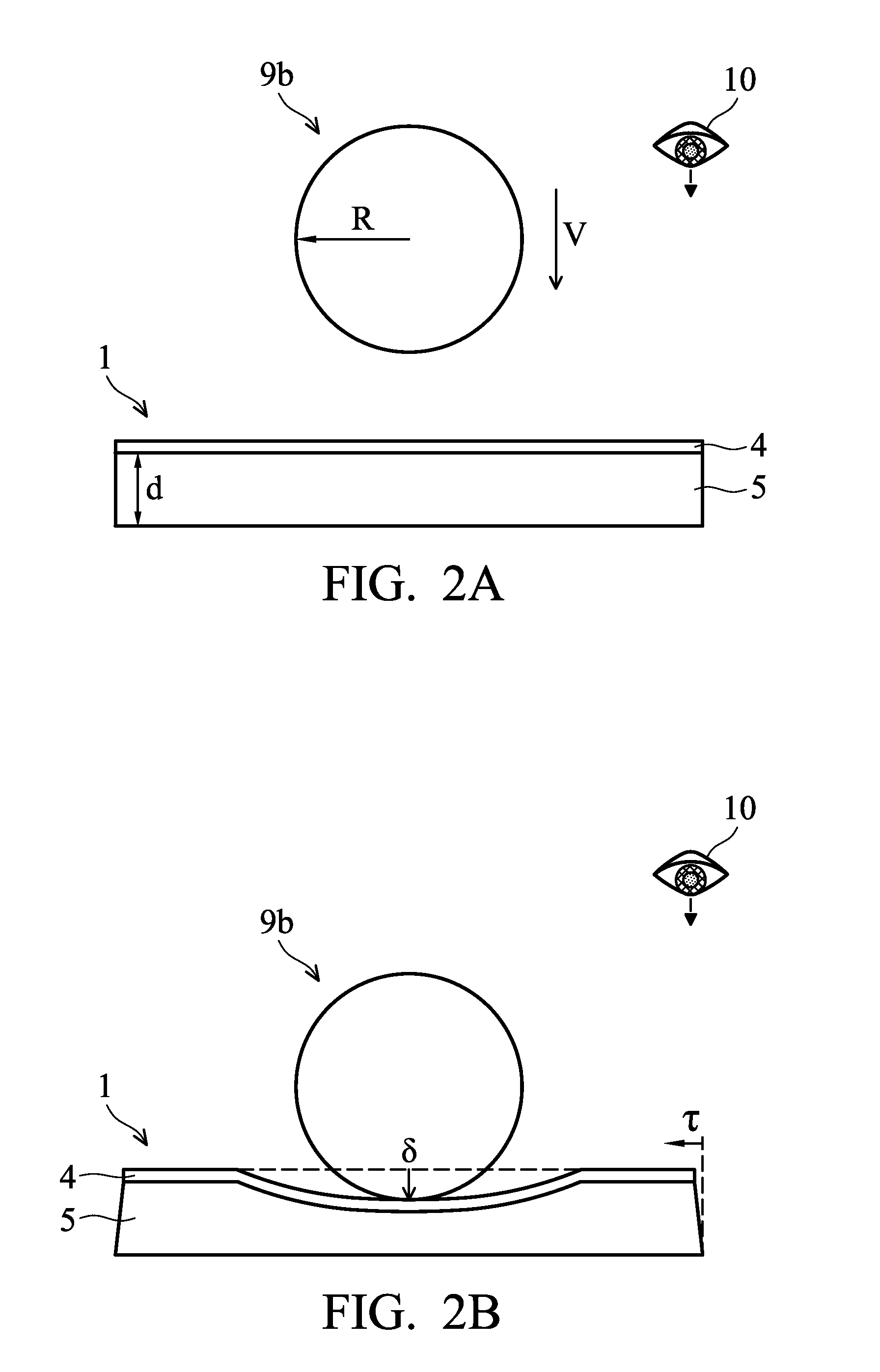
[0034]The following description of certain exemplary embodiments and model equations is merely exemplary in nature and is in no way intended to limit the invention, its application, or uses. In the following detailed description of embodiments of the present systems, devices and methods, reference is made to the accompanying drawings which form a part hereof, and in which are shown by way of illustration specific embodiments in which the described devices and methods may be practiced. These embodiments are described in sufficient detail to enable those skilled in the art to practice the presently disclosed systems and methods, and it is to be understood that other embodiments may be utilized and that structural and logical changes may be made without departing from the spirit and scope of the present system. The following detailed description is therefore not to be taken in a limiting sense, and the scope of the present system is defined only by the appended claims. Moreover, for th...


PUM

PropertyMeasurementUnit
Lengthaaaaaaaaaa
Viscosityaaaaaaaaaa
Viscosityaaaaaaaaaa

Abstract

An impact resistant device includes an optical layer and electronics. The optical layer and electronics are comprised in a flexible foil structure which is supported by a backing structure in mechanical contact on a backside of the flexible foil structure. The backing structure includes a deformable material having a viscous response in a critical range, which critical range is defined for a given front impact event by a pressure threshold (σcritical) and a stretching threshold (εcritical) of the flexible foil structure such that the optical layer and / or electronics are not damaged by the impact event.

Description

[0001]This application claims the benefit of U.S. Provisional Application Ser. No. 61 / 512,955, filed on Jul. 29, 2011, which is hereby incorporated by reference.TECHNICAL FIELD AND BACKGROUND[0002]The present invention relates to an impact resistant device comprising an optical layer such as an impact resistant display device.[0003]The term “impact resistance” is used hereinafter to refer to the desired ability of a device or layer to resist a certain impact, e.g. as a result of a projectile or fall of the device, while still maintaining normal functionality after the impact. The term “impact” is defined hereinafter as a collision of an object with the device at a relative velocity of more than 0.1 m / s. The term “optical layer” is used hereinafter to refer to a layer or combination of layers that provides a functional effect when electromagnetic radiation, in particular light of optical frequencies, is absorbed, emitted, or transmitted by the optical layer. Active functional effects...

Claims


Application Information

Patent Timeline
IPC IPC(8): B32B27/40B32B7/02H05K5/00B23P17/04G06F3/038B32B3/26H01L31/048
CPCB32B27/065B32B27/40H01L31/0481Y10T428/24942Y02E10/52H02S30/20Y10T29/49826H01L31/1876Y02E10/50Y02P70/50Y10T428/24998Y10T428/31551
Inventor BOUTEN, LUCAS MARTINUSSCHELLEKENS, MICHIEL ADRIANUS JOHANNES H. J.VAN VEENENDAAL, ERIKHUITEMA, HJALMAR EDZER AYCO
Owner SAMSUNG ELECTRONICS CO LTD
Learn More