A fully automatic silicon wafer intelligent flip stacking double-chip inserting machine

A fully automatic, inserting machine technology, applied in the direction of conveyors, conveyor objects, final product manufacturing, etc., can solve the problems of scratching the surface of the main body of the silicon wafer, affecting the accuracy of insertion and positioning, and affecting the accuracy of the surface of the main body of the silicon wafer. , to achieve the effect of improving the feeding suitability of inserting sheets, improving the safety of inserting sheets, and ensuring the efficiency of inserting sheets

Active Publication Date: 2021-12-03
江苏泰明易自动化设备有限公司
View PDF4 Cites 0 Cited by
  • Summary
  • Abstract
  • Description
  • Claims
  • Application Information

AI Technical Summary

Problems solved by technology

[0004] The purpose of the present invention is: in order to solve the problem that it is easy to scratch the surface of the main body of the silicon wafer when grasping, which affects the accuracy of insertion and positioning, and it is easy to affect the quasi-precision of the surface of the main body of the silicon wafer due to impurities on the bonding surface when grasping, and A fully automatic silicon wafer intelligent flip-stack double-wafer insertion machine proposed

Method used


Image

  • A fully automatic silicon wafer intelligent flip stacking double-chip inserting machine
  • A fully automatic silicon wafer intelligent flip stacking double-chip inserting machine
  • A fully automatic silicon wafer intelligent flip stacking double-chip inserting machine

Examples


Embodiment Construction

[0041]The following will clearly and completely describe the technical solutions in the embodiments of the present invention with reference to the accompanying drawings in the embodiments of the present invention. Obviously, the described embodiments are only some, not all, embodiments of the present invention. Based on the embodiments of the present invention, all other embodiments obtained by persons of ordinary skill in the art without creative efforts fall within the protection scope of the present invention.

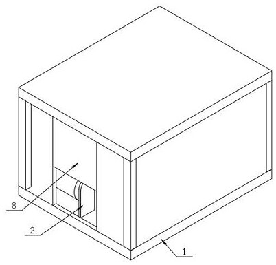
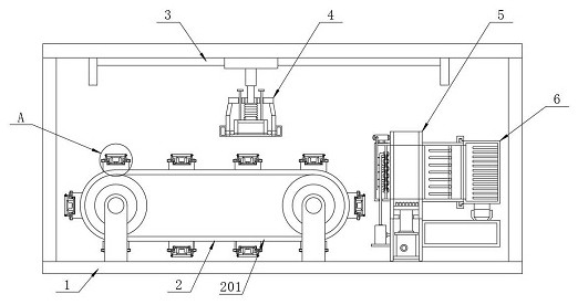
[0042] see Figure 1-8 , the present invention provides a technical solution: a fully automatic silicon wafer intelligent flip stacking double-chip inserting machine, including a base 1, and a feeding mechanism 2 is fixedly installed at the bottom of the inner cavity of the base 1 to transport the main body of the silicon wafer 208, a linear module 3 is fixedly installed on the top of the inner cavity of the base 1, and a grasping mechanism 4 is fixedly installed on...


PUM


Abstract

The invention discloses a full-automatic silicon wafer intelligent flip stacking double-chip inserting machine, which belongs to the technical field of silicon wafer production and includes a base. The top of the inner cavity of the base is fixedly equipped with a linear module, and the bottom of the linear module is fixedly equipped with a grabbing mechanism for grabbing the main body of the silicon wafer and transporting the material. One side of the top of the base is fixedly connected with an insert mechanism. In the present invention, the main body of the silicon wafer in the feeding trough is moved by the flow of the ejected liquid through the pressurized nozzle on one side, and the impact force of the medium circulation can drive the main body of the silicon wafer that falls into it through the guide plate on one side and insert it in the In the slot of the inserting fixture, when the inserting process of the main body of the silicon wafer can be realized under the action of the fluid, on the one hand, the efficiency of the inserting can be guaranteed, and on the other hand, the safety of the inserting can be simultaneously improved, and the main body of the silicon wafer can be avoided due to contact friction of the inserting mechanism. The wear of the surface meets the needs of the insert processing.

Description

technical field [0001] The invention belongs to the technical field of silicon wafer production, in particular to a fully automatic silicon wafer intelligent flip stacking double-chip inserting machine. Background technique [0002] In order to meet the needs of sustainable development, the utilization of solar energy has been gradually paid attention to. As an important component of solar cells, silicon wafers need to be cut and stacked during silicon wafer processing. Inserting the cut and stacked silicon wafers into the basket is generally done The way of manual pick and place or suction cup grabbing. [0003] However, in actual processing and use, the efficiency of manual pick-and-place or grasping inserts is low, and at the same time affects the accuracy of insertion positioning, the impurities on the bonding surface cannot be removed well, and it is easy to scratch the silicon due to the impurity airflow impact At the same time, it is easy to cause damage due to conta...

Claims


Application Information

Patent Timeline
Patent Type & Authority Patents(China)
IPC IPC(8): H01L21/677H01L31/18B65G15/58B65G47/91
CPCH01L21/67781H01L21/67766H01L31/1804B65G47/912B65G15/58Y02P70/50
Inventor 冯显火
Owner 江苏泰明易自动化设备有限公司
Why Eureka
Try Eureka