Glass substrate for forming through-substrate via of semiconductor device

a glass substrate and semiconductor technology, applied in semiconductor devices, thin material processing, basic electric elements, etc., can solve the problems of wire-bonding technology not being able to cope with the narrow pitch, glass substrate may break relatively easily, break or crack may easily occur, etc., to achieve satisfactory strength

Inactive Publication Date: 2013-02-07
ASAHI GLASS CO LTD
View PDF2 Cites 68 Cited by
  • Summary
  • Abstract
  • Description
  • Claims
  • Application Information

AI Technical Summary

Benefits of technology

[0011]The present invention is conceived in view of the above problem, and one object of an embodiment is to provide a glass substrate having a more satisfactory strength compared to the conventional glass substrate for forming the through-substrate via of the semiconductor device.

Problems solved by technology

In this case, the wire-bonding technology is unable to cope with the narrow pitch, and an interposing substrate called an interposer using through-substrate vias may be required.
However, in such a glass substrate for forming the through-substrate via of the semiconductor device, there may be a problem in that a break or crack may easily occur in an outer peripheral part of an opening of a penetration hole (that is, at an interface of the penetration hole and a non-opening part) at the surface of the glass substrate.
For example, there is a possibility that the crack may occur in the glass substrate for forming the through-substrate via of the semiconductor device even when a bending stress received thereby is small, from an origin formed by the outer peripheral part, and the glass substrate may break relatively easily.
When such a tendency continues, the strength of the glass substrate may deteriorate further, and for this reason, the above described problem of the crack occurring at the outer peripheral part of the penetration hole may become more notable.

Method used


Image

  • Glass substrate for forming through-substrate via of semiconductor device
  • Glass substrate for forming through-substrate via of semiconductor device
  • Glass substrate for forming through-substrate via of semiconductor device

Examples


example 1

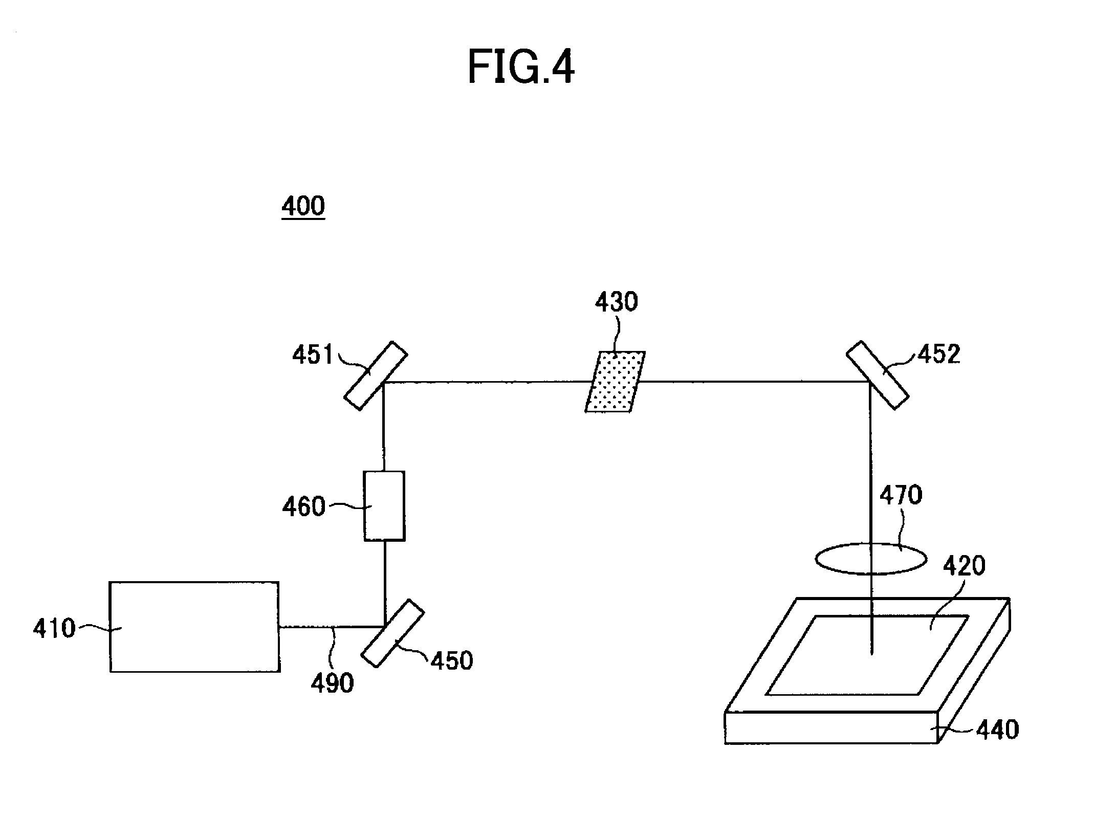
[0108]The glass substrate having the plurality of penetration holes is manufactured according to the following procedures, using the manufacturing apparatus illustrated in FIG. 4.

[0109](Manufacturing Glass Substrate)

[0110]First, a plate-shaped glass is formed according to the following procedures.

[0111]Each raw material powder is weighed and mixed in order to obtain 1 kg of a mixed powder that includes 72.8 wt % of SiO2, 1.9 wt % of Al2O3, 3.7 wt % of MgO, 8.1 wt % of CaO, 13.1 wt % of Na2O, and 0.3 wt % of K2O. In addition, sodium sulfate is added to become 0.4 wt % in SO3—equivalent content. Next, the mixed powder is put into a platinum crucible and maintained at 1600° C. for 3 hours, in order to melt the mixed powder. The melted material is subjected to a degassing process and homogenized, before flowing the melted material into a mold. Thereafter the mold is slowly cooled, in order to obtain a glass sample.

[0112]The glass sample that is obtained is cut and polished into a size h...

example 2

[0135]A glass substrate having a large number of penetration holes is formed by a method similar to that for the Example 1, and the chemical strengthening process is performed on the glass substrate.

[0136]However, in an Example 2, the composition of the plate-shaped glass is 60.9 wt % of SiO2, 9.6 wt % of Al2O3, 7.0 wt % of MgO, 11.7 wt % of Na2O, 5.9 wt % of K2O, and 4.8 wt % of ZrO2. No Cao is added. Other manufacturing conditions of the plate-shaped glass are similar to those of the Example 1.

[0137]The Table 1 illustrates the composition and various characteristics of the glass substrate in a row of the “Example 2”. The density is 2.52 g / cm3 and the Young's modulus is approximately 78 GPa for the glass substrate that is obtained. In addition, the average coefficient of thermal expansion of the glass substrate is 91×10−7 / K at 50° C. to 350° C. Further, the glass transition temperature is 620° C., and the strain point is 578° C.

[0138]Moreover, the conditions of the laser beam machi...

example 3

[0142]A glass substrate having a large number of penetration holes is formed by a method similar to that for the Example 1, and the chemical strengthening process is performed on the glass substrate.

[0143]However, in an Example 3, the composition of the plate-shaped glass is 62.2 wt % of SiO2, 17.2 wt % of Al2O3, 3.9 wt % of MgO, 0.6 wt % of CaO, 12.8 wt % of Na2O, and 3.5 wt % of K2O. No ZrO2 is added. Other manufacturing conditions of the plate-shaped glass are similar to those of the Example 1.

[0144]The Table 1 illustrates the composition and various characteristics of the glass substrate in a row of the “Example 3”. The density is 2.46 g / cm3 and the Young's modulus is approximately 73 GPa for the glass substrate that is obtained. In addition, the average coefficient of thermal expansion of the glass substrate is 93×10−7 / K at 50° C. to 350° C. Further, the glass transition temperature is 595° C., and the strain point is

[0145]553° C.

[0146]Moreover, the conditions of the laser beam...


PUM

PropertyMeasurementUnit
thicknessaaaaaaaaaa
thicknessaaaaaaaaaa
surface compressive stressaaaaaaaaaa

Abstract

A glass substrate for forming a through-substrate via of a semiconductor device includes a first surface and a second surface, and penetration holes extending from the first surface to the second surface, wherein at least one of the first and second surfaces is chemically strengthened.

Description

CROSS-REFERENCE TO RELATED APPLICATIONS[0001]This application is a continuation application filed under 35 U.S.C. 111(a) claiming the benefit under 35 U.S.C. 120 and 365(c) of a PCT International Application No. PCT / JP2011 / 059317 filed on Apr. 14, 2011, which is based upon and claims the benefit of priority of the prior Japanese Patent Application No. 2010-097225 filed on Apr. 20, 2010, the entire contents of which are incorporated herein by reference.BACKGROUND OF THE INVENTION[0002]1. Field of the Invention[0003]The present invention relates to a glass substrate for forming a through-substrate via of a semiconductor device.[0004]2. Description of the Related Art[0005]In order to cope with demands to increase the integration density of the printed circuit board due to high-density packaging, a multi-layer printed circuit board was developed in which a plurality of printed circuit boards are stacked. In such a multi-layer printed circuit board, micro penetration holes having a diame...

Claims


Application Information

Patent Timeline
Patent Type & Authority Applications(United States)
IPC IPC(8): B32B3/24B32B17/06
CPCH01L23/15H01L23/49827H01L21/4807Y10T428/24273H01L2924/0002Y10T428/24298H01L2924/00
Inventor KOIKE, AKIOONO, MOTOSHIMURAKAMI, RYOTAKIKUGAWA, SHINYA
Owner ASAHI GLASS CO LTD
Why Eureka
Try Eureka