Touch panel and manufacturing method thereof

a technology of capacitive touch panel and manufacturing method, which is applied in the direction of superimposed coating process, liquid/solution decomposition chemical coating, instruments, etc., can solve the problem of inability to normal operation of the touch panel, and achieve the effect of avoiding fluctuation of resistance value and avoiding mutual conduction of circuits

Active Publication Date: 2013-02-21
TPK TOUCH SOLUTIONS (XIAMEN) INC
View PDF2 Cites 47 Cited by
  • Summary
  • Abstract
  • Description
  • Claims
  • Application Information

AI Technical Summary

Benefits of technology

[0033]Based on the above-mentioned disclosure for the touch panel, touch structures in the touch area, periphery area, and icon area have effects of maintaining insulating performance of the shielding layer and insulation bridge in the insulation layer, avoiding fluctuation of resistance value in the electrode layer and avoiding mutual conduction of the circuits in the circuit layer.

Problems solved by technology

This, in turn, makes wires of the circuit layer 400 electrically connect to each other leading to incapability of normal operation of the touch panel.

Method used


Image

  • Touch panel and manufacturing method thereof
  • Touch panel and manufacturing method thereof
  • Touch panel and manufacturing method thereof

Examples


first embodiment

The First Embodiment

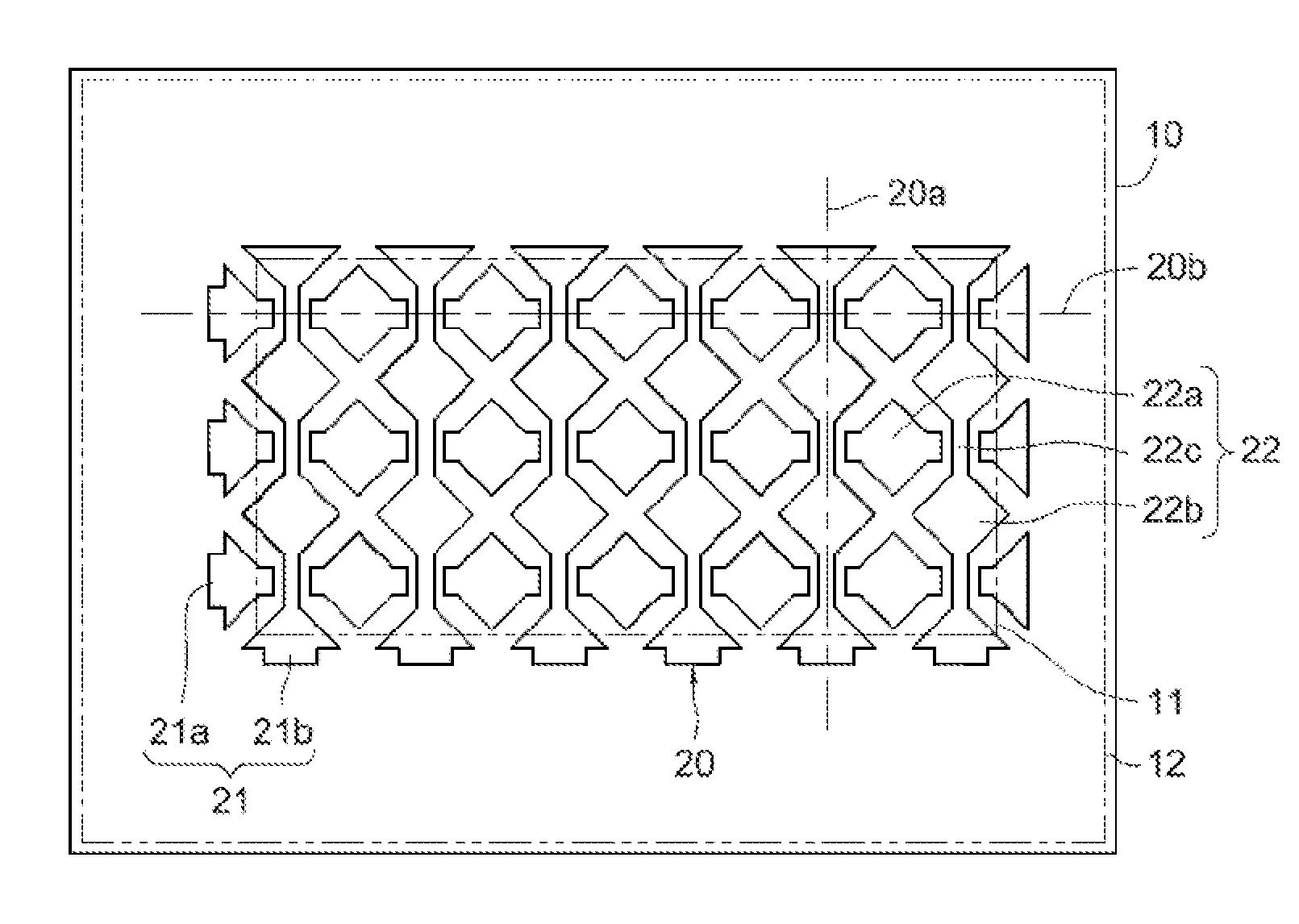
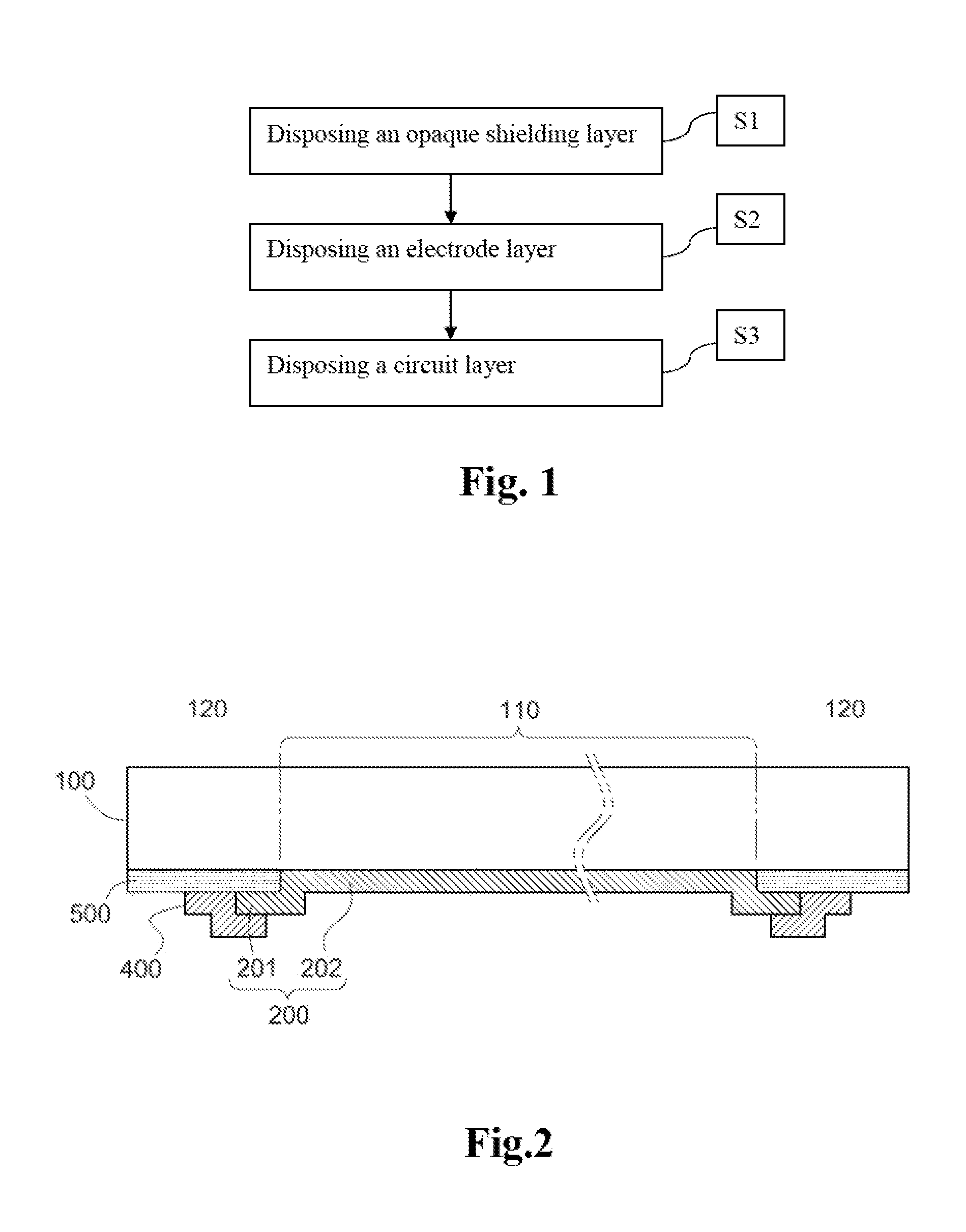
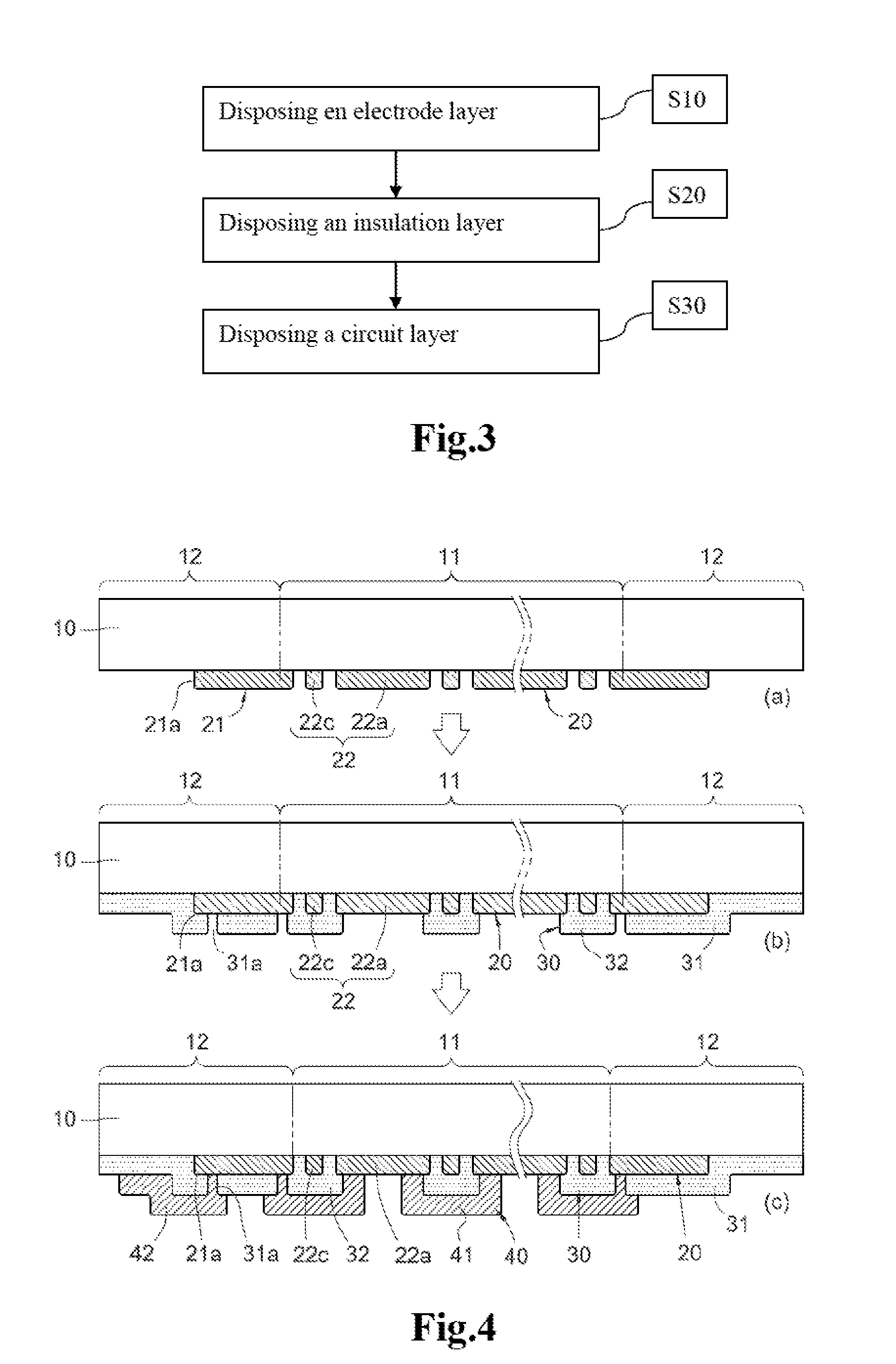
[0040]In view of carrying out the manufacturing method for touch panel in accordance with the present disclosure, particularly relating to the manufacturing method for a capacitive touch panel, refer to FIG. 3 to FIG. 7. FIG. 3 discloses a block flowchart of the manufacturing method in accordance with the present invention; FIG. 4(a) to FIG. 4(c) are schematic sectional views of the touch panel of the present diclosure in disposition process disclosed one by one according to the method of FIG. 3; FIG. 5 to FIG. 7 are plan bottom views of the structure according to each view of FIG. 4(a) to FIG. 4(c). Manufacturing method for the touch panel comprises: step S10, first disposing an electrode layer 40, extending an overlapping electrode 21 from touch area 11 of a substrate 10 to periphery area 12 of the substrate 10 so that electrical signals of the touch area 11 will be transmitted to an external control circuit through the overlapping electrode 21, wherein the per...

second embodiment

The Second Embodiment

[0066]FIG. 8 to FIG. 10 disclose plan bottom views of the touch structure formed in an icon area 13 of the present disclosure in the process of disposing the electrode layer 20, the insulation layer 30 and the circuit layer 40, illustrating that in a specific embodiment of the manufacturing method, the substrate 10 further comprises an icon area 13 preset within the region scope of the periphery area 12.

[0067]In step S10, especially in the step of forming the overlapping electrodes 21 and the sensing electrodes 22, the electrode layer 20 can simultaneously be disposed to form an independent end electrode 26, an independent sub-electrode 27, a serially-connected sub-electrode 28, and a sub connection line 29 extending from the serially-connected electrode 22b to the icon area 13, wherein the serially-connected sub-electrode 28 and the serially-connected electrode 22b are serially and electrically connected by the sub connection line 29. Mutually insulated indepen...


PUM

PropertyMeasurementUnit
temperatureaaaaaaaaaa
heat resistanceaaaaaaaaaa

Abstract

The present disclosure provides a manufacturing method for a touch panel comprising: disposing an electrode layer extending from touch area of a substrate to periphery area of the substrate, wherein the periphery area surrounds the periphery of the touch area. The method further includes disposing an insulation layer in the periphery area of the substrate to form a shielding layer, making the shielding layer cover the overlapping electrode in the periphery area and making the electrode layer of the touch area and the overlapping electrode locate on the same layer of the substrate so as to avoid fluctuation of resistance value in the electrode layer due to height difference. Meanwhile, adopting the disposition method also maintains insulating performance of the shielding layer. The present disclosure also provides a touch panel made by the manufacturing method.

Description

BACKGROUND OF THE INVENTION[0001]This Application claims the benefit of the People's Republic of China Application No. 201110270292.7; filed on Aug. 17, 2011.FIELD OF THE INVENTION[0002]The present disclosure relates to a touch panel and a manufacturing method thereof, and more particularly to a capacitive touch panel and manufacturing method thereof.DESCRIPTION OF THE RELATED ART[0003]Touch panel is a platy structure object, usually configured in electronic touch devices such as LCD screens.[0004]Referring to FIG. 1 and FIG. 2, FIG. 1 is a block flowchart of a manufacturing method for a conventional touch panel and FIG. 2 is a schematic sectional view of a conventional touch panel.[0005]Step S1: disposing an opaque shielding layer 500 in periphery area 120 of a substrate 100;[0006]Step S2: disposing an electrode layer 200 on the substrate 100. The electrode layer 200 comprises a sensing electrode 202 directly formed in the touch area 110 of the substrate 100 and an overlapping elec...

Claims


Application Information

Patent Timeline
Patent Type & Authority Applications(United States)
IPC IPC(8): H05K1/11H05K3/46H05K1/00
CPCG06F3/044G06F3/047G06F2203/04111G06F2203/04103G06F3/0443G06F3/0446G06F3/041G06F2203/04107
Inventor XIE, YANJUNHO, KWAN-SIN
Owner TPK TOUCH SOLUTIONS (XIAMEN) INC
Why Eureka
Try Eureka