LOW TEMPERATURE MIGRATION ENHANCED Si-Ge EPITAXY WITH PLASMA ASSISTED SURFACE ACTIVATION

a low temperature migration and surface activation technology, applied in the direction of polycrystalline material growth, chemically reactive gas growth, crystal growth process, etc., can solve the problems of high production cost and system cost of communication networks using such devices, incompatibility with high volume, and inability to benefit from the economies of scale achieved

Inactive Publication Date: 2013-02-21
INTERMOLECULAR
View PDF6 Cites 8 Cited by
  • Summary
  • Abstract
  • Description
  • Claims
  • Application Information

AI Technical Summary

Problems solved by technology

Typically, these material systems are not compatible with high volume, Si-based CMOS manufacturing processes and cannot benefit from the economies of scale that have been achieved therein.
Therefore, the manufacturing cost and systems cost for communication networks using such devices remains high and limits the adoption and deployment of such networks.
However, at high Ge concentrations and higher temperatures typically used for the thermally activated growth of Si—Ge alloys, the films relax at a critical thickness resulting in a highly defective film.
Additionally, Ge tends to segregate or cluster within the film, forming a non-uniform and highly defective film.
Other disadvantages of high temperature growth include dopant redistribution, dopant surface segregation, autodoping, and incompatibility with low temperature substrates such as thin film solar cells, thin film transistors, polymers, etc.
These disadvantages reduce the mobility of the carriers within the device channel and lower the device speed.
Simply lowering the growth temperature to about 550 C results in issues such as a slow deposition rate, and high defect density.
These various species can interact in the gas phase through unwanted reactions and can form particulate matter that is deposited on the substrate rather than forming the desired film through well controlled surface reactions.
Therefore, PECVD has many challenges when applied to the epitaxial growth of Si, Ge, and / or Si—Ge alloys.

Method used


Image

  • LOW TEMPERATURE MIGRATION ENHANCED Si-Ge EPITAXY WITH PLASMA ASSISTED SURFACE ACTIVATION
  • LOW TEMPERATURE MIGRATION ENHANCED Si-Ge EPITAXY WITH PLASMA ASSISTED SURFACE ACTIVATION

Examples


Embodiment Construction

[0012]A detailed description of one or more embodiments is provided below along with accompanying figures. The detailed description is provided in connection with such embodiments, but is not limited to any particular example. The scope is limited only by the claims and numerous alternatives, modifications, and equivalents are encompassed. Numerous specific details are set forth in the following description in order to provide a thorough understanding. These details are provided for the purpose of example and the described techniques may be practiced according to the claims without some or all of these specific details. For the purpose of clarity, technical material that is known in the technical fields related to the embodiments has not been described in detail to avoid unnecessarily obscuring the description.

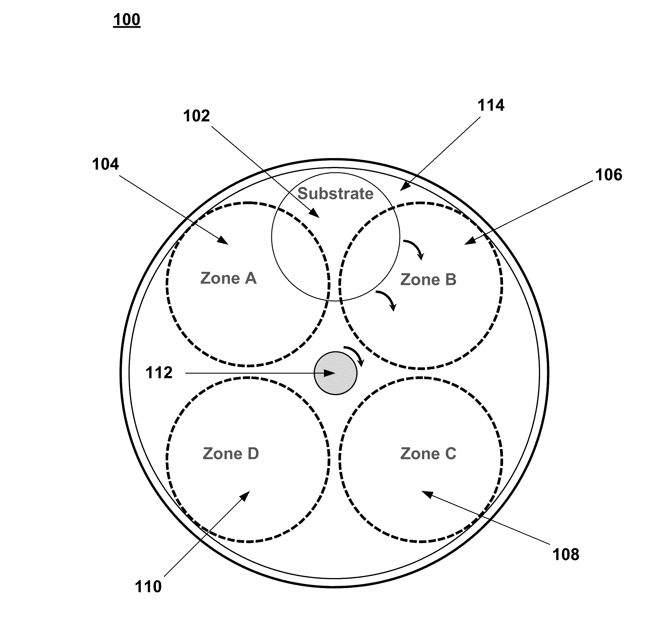
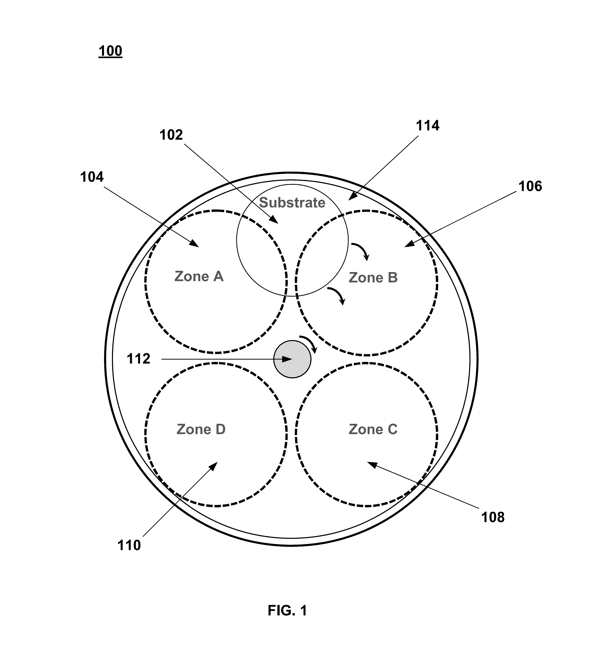
[0013]The epitaxial growth of Si from silane has been well characterized. At low temperatures, the deposition proceeds through a number of surface reactions as illustrated in ...


PUM

PropertyMeasurementUnit
frequenciesaaaaaaaaaa
thicknessaaaaaaaaaa
rotation speedaaaaaaaaaa

Abstract

Epitaxial films are grown by alternately exposed to precursor dosing regions, inert gas plasma regions, hydrogen-containing plasma regions, chlorine-containing plasma and metrology regions, or regions where an atomic hydrogen source is located. Alternately, laser irradiation techniques may be substituted for the plasma energy in some of the processing regions. The film growth process can be implemented at substrate temperatures between about 25 C and about 600 C, together with optional exposures to laser irradiation to cause the surface of the film to melt or to experience a near-melt condition.

Description

FIELD OF THE INVENTION[0001]The present invention relates generally to methods and apparatus for forming epitaxial Si, Ge, or Si—Ge alloy films at low temperatures.BACKGROUND OF THE INVENTION[0002]Semiconductor devices with high carrier mobility are required for high speed communications in frequency ranges from about 1 giga-hertz (GHz) to about 100 GHz. Expensive compound semiconductor materials systems such as InP, GaAs, and GaN are often used for such devices. Typically, these material systems are not compatible with high volume, Si-based CMOS manufacturing processes and cannot benefit from the economies of scale that have been achieved therein. Therefore, the manufacturing cost and systems cost for communication networks using such devices remains high and limits the adoption and deployment of such networks.[0003]Semiconductor devices with semiconductor layers based on strained silicon and / or Si—Ge alloys exhibit properties that are suitable for use in communication networks at ...

Claims


Application Information

Patent Timeline
Patent Type & Authority Applications(United States)
IPC IPC(8): H01L21/20
CPCH01L21/02532H01L21/0262C23C16/42C23C16/4554C23C16/483C30B25/12C30B29/06C30B29/08C23C16/45551
Inventor KRAUS, PHILIP A.PRAMANIK, DIPANKARBORISOV, BORIS
Owner INTERMOLECULAR
Why Eureka
Try Eureka