Method of forming conformal dielectric film having Si-N bonds by PECVD

a dielectric film and conformal technology, applied in the direction of semiconductor/solid-state device details, chemical vapor deposition coatings, coatings, etc., can solve the problems of poor conformality or poor step coverage on a substrate containing small and/or high aspect ratio features, poor conformal coverage can hamper the development of higher density circuit devices and elements, and extremely poor deposition rates

Active Publication Date: 2011-07-05
ASM JAPAN
View PDF18 Cites 423 Cited by
  • Summary
  • Abstract
  • Description
  • Claims
  • Application Information

AI Technical Summary

Benefits of technology

[0011]Another object of at least one embodiment of the present invention is to provide a method for modifying etch properties of the deposited layers, such as wet etching rates, by adding a second precursor while maintaining high deposition rates and high conformality. In some embodiments, the conformal dielectric film is a carbon-doped silicon nitride having a carbon concentration of at least about 5% (e.g., 20% to 40%) and having a dielectric constant of about 7 or lower (e.g., 5.5 to 7).
[0015]In an embodiment, the hydrogen-containing silicon gas may have no carbon atom in its molecule and may constitute a first precursor, and the precursor may further comprise a hydrocarbon-containing gas as a second precursor. By adding the second precursor, the wet etching rate of the resultant film, for example, can significantly be improved or manipulated.
[0021]In some embodiments, the method further comprise, after forming the conformal dielectric film as a first conformal dielectric film, increasing the pulse duration of the second precursor per cycle without changing the length of one cycle which is the same as that for the first precursor, or performing multiple cycles of the second precursor per one cycle of the first precursor, thereby forming a second conformal dielectric film which has a carbon concentration higher than that of the first conformal dielectric film.

Problems solved by technology

However, the PECVD method for forming silicon nitride leads to poor conformality or poor step coverage on a substrate containing small and / or high aspect ratio features.
In small circuits and devices, such as ultra-large scale integrated (ULSI) circuitry, poor conformal coverage can hamper the development of higher density circuit devices and elements.
However, the ALD method for forming silicon nitride leads to extremely poor deposition rates.
Such poor deposition rates hamper the manufacturing cost down for development of higher density circuit devices and elements.
The second precursor may have no silane from the point of view that it is not easy to control the carbon concentration of the resultant conformal dielectric film by using a precursor containing silane as compared with using a precursor of hydrocarbon containing no silane.

Method used


Image

  • Method of forming conformal dielectric film having Si-N bonds by PECVD
  • Method of forming conformal dielectric film having Si-N bonds by PECVD
  • Method of forming conformal dielectric film having Si-N bonds by PECVD

Examples


example 1

No Second Precursor

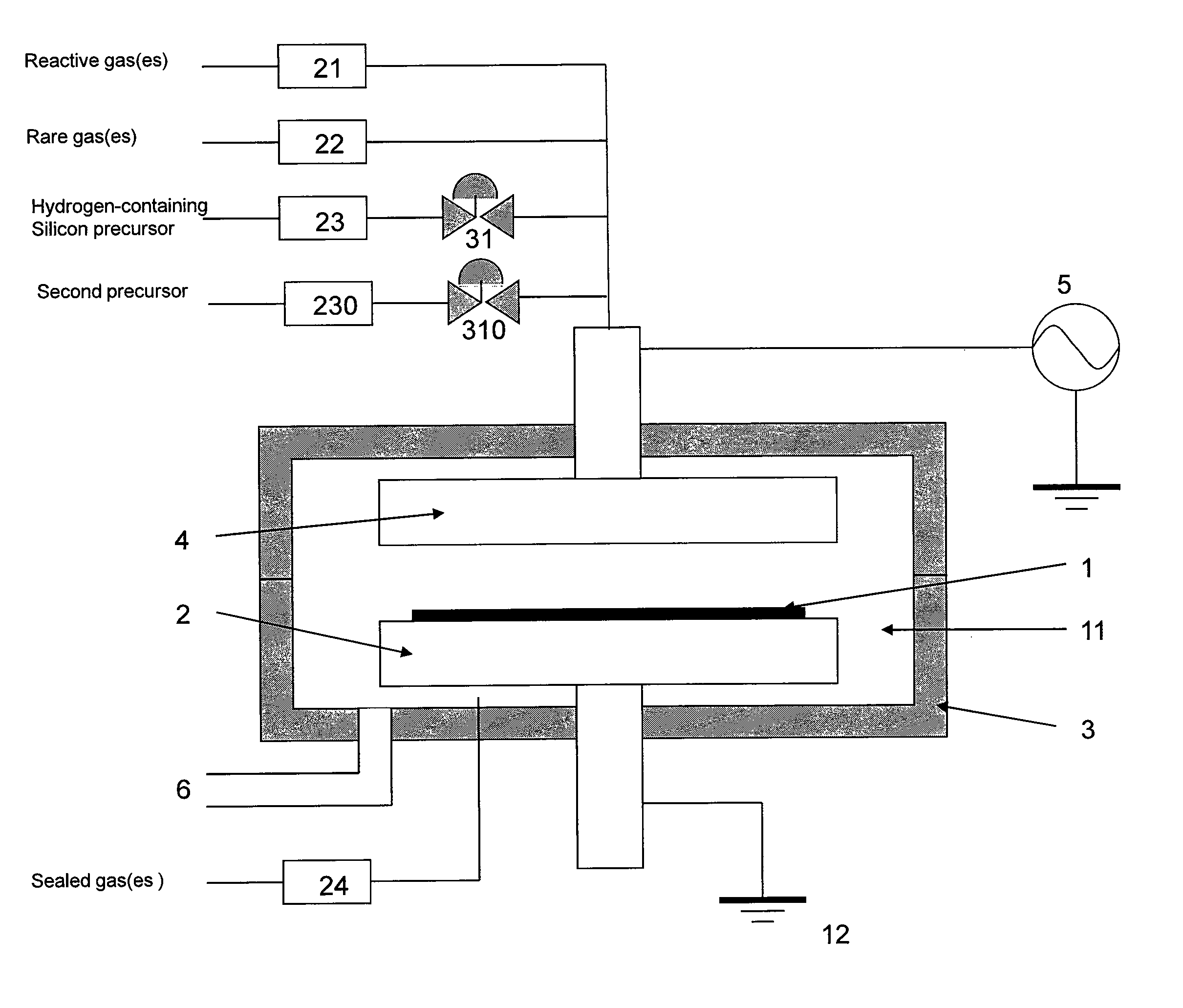
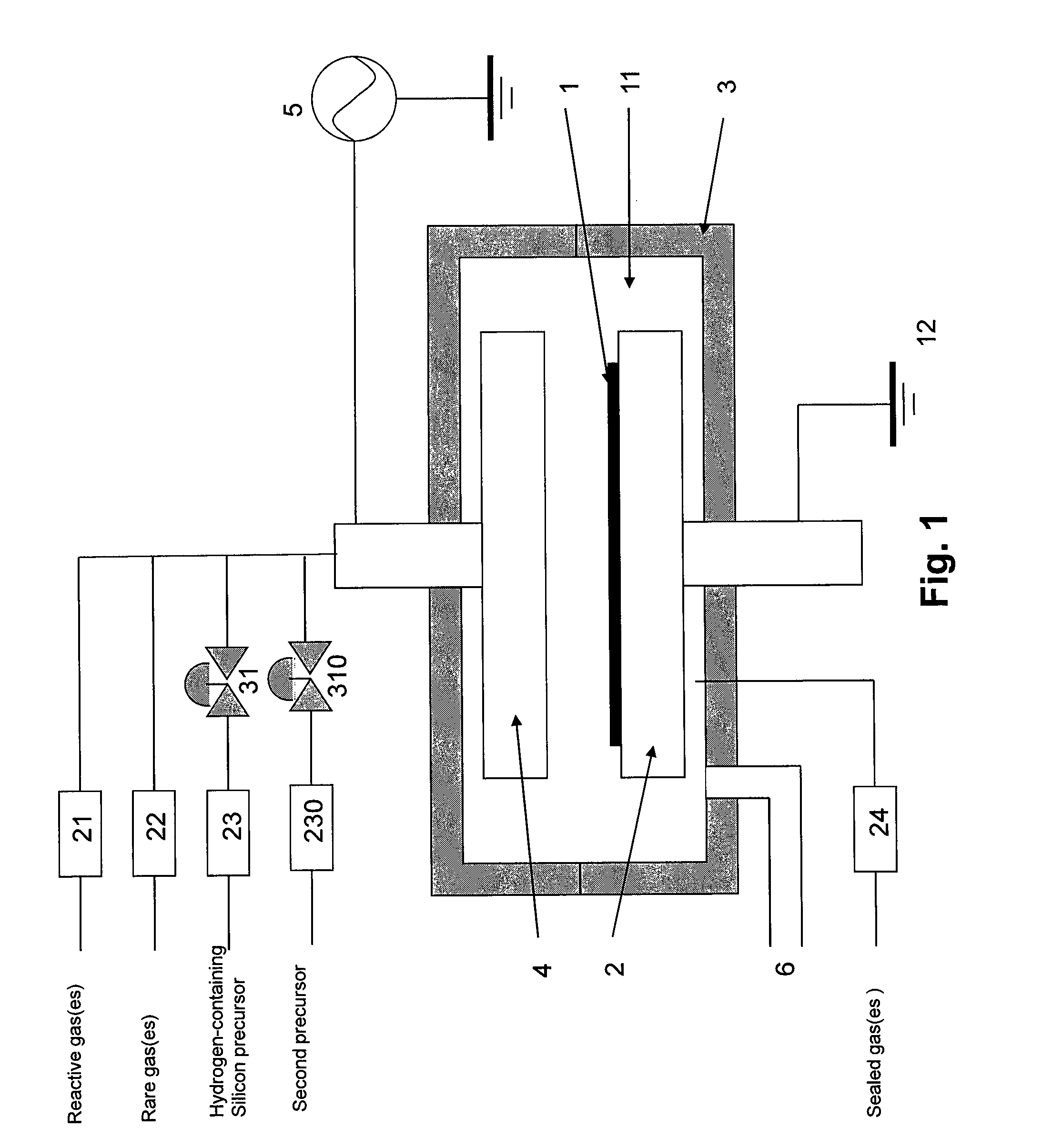
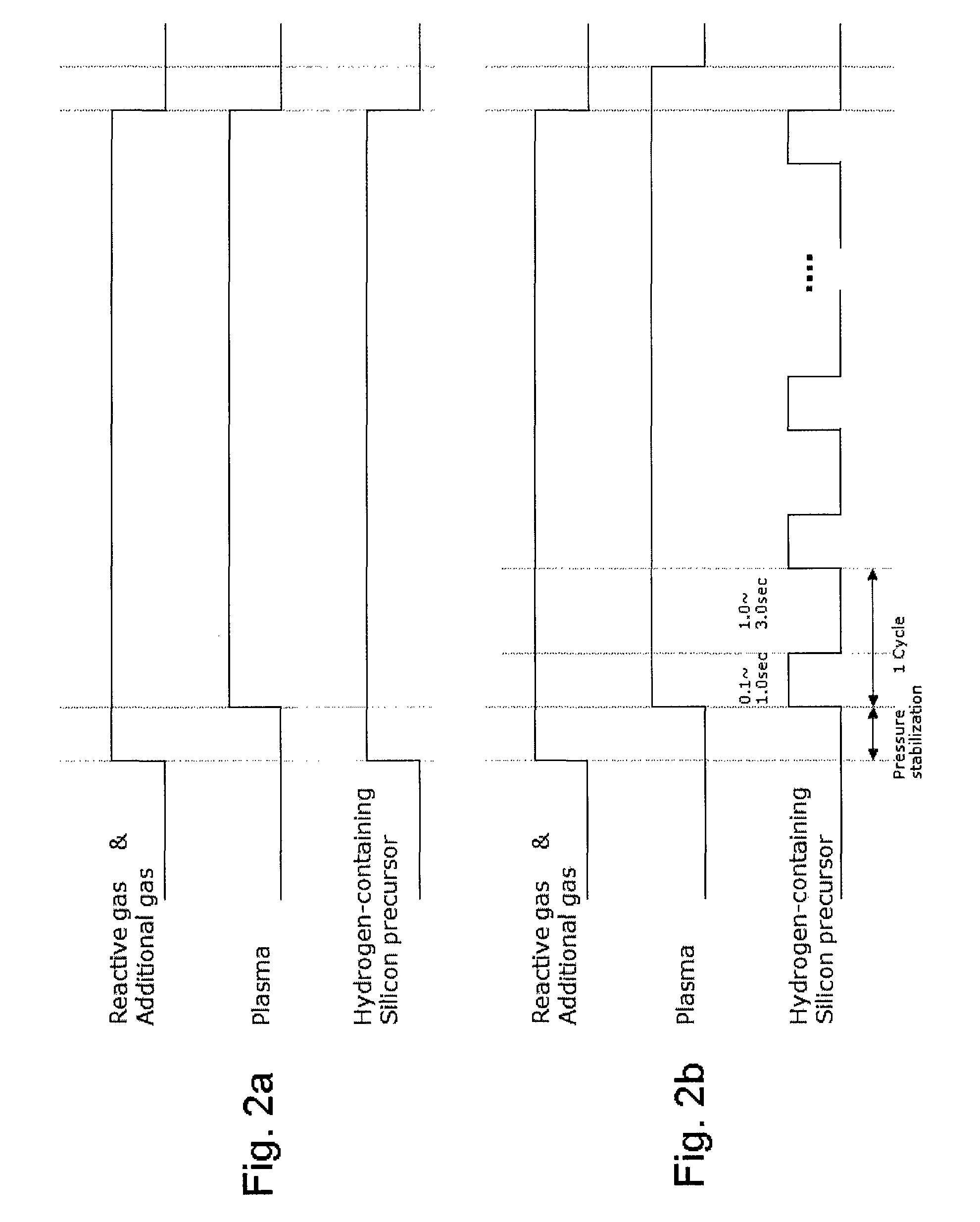
[0130]An insulative silicon nitride layer was formed on a substrate having trenches under the conditions shown below using the sequence illustrated in FIG. 2b and the PECVD apparatus illustrated in FIG. 1. The trenches included relatively wide trenches (a width of 500 nm and a depth of 350 nm) and relatively narrow trenches (a width of 50 nm and a depth of 350 nm). Thus trenches of different aspect ratio were coated.

[0131]Silane: 50 sccm

[0132]Hydrogen: 1000 sccm

[0133]Nitrogen: 2000 sccm

[0134]Process helium: 2000 sccm

[0135]Sealed helium: 500 sccm

[0136]Argon: 100 sccm

[0137]Substrate Temp.: 300° C.

[0138]RF power (a frequency of 13.56 MHz): 0.12 W / cm2

[0139]Pressure: 6 Ton

[0140]Silane supply time: 1 sec supply, 3 sec supply stop

[0141]After completion of the deposition, the trenches were observed with a scanning electron microscope.

[0142]It was confirmed that the step coverage (conformality) was more than 80% (80%-87%), defined as the ratio between the thickness of the...

example 2

No Second Precursor

[0143]An insulative silicon nitride layer was formed on a substrate having trenches under the conditions shown below using the sequence illustrated in FIG. 2b and the PECVD apparatus illustrated in FIG. 1. The trenches included relatively wide trenches (a width of 500 nm and a depth of 350 nm) and relatively narrow trenches (a width of 50 nm and a depth of 350 nm).

[0144]Trisilylamine: 300 sccm

[0145]Hydrogen: 500 sccm

[0146]Nitrogen: 1000 sccm

[0147]Process helium: 1400 sccm

[0148]Sealed helium: 500 sccm

[0149]Argon: 500 sccm

[0150]Substrate temp.: 300° C.

[0151]RF power (a frequency of 13.56 MHz): 0.12 W / cm2

[0152]Pressure: 6 Torr

[0153]Trisilylamine supply time: 0.2 sec supply, 2 sec supply stop

[0154]After completion of the deposition, the trenches were observed with a scanning electron microscope (SEM).

[0155]FIGS. 3a and 3b show the scanning electron microscope cross-sectional view of the substrate with the conformal silicon nitride layer formed. Qualitatively, the sili...

example 3

No Second Precursor

[0157]A dielectric layer was formed without an additive precursor on a substrate under the conditions shown below based on the sequence illustrated in FIG. 5.

[0158]Trisilylamine: 100 sccm

[0159]Hydrogen: 500 sccm

[0160]Nitrogen: 1000 sccm

[0161]Process helium: 1400 sccm

[0162]Sealed helium: 500 sccm

[0163]Argon: 1000 sccm

[0164]Substrate temperature: 400° C.

[0165]High frequency RF power (a frequency of 13.56 MHz): 0.07 W / cm2

[0166]Low frequency RF power (a frequency of 430 kHz): 0.0 W / cm2

[0167]Trisilylamine supply time: 0.3 sec supply, 2.0 sec supply stop

[0168]In this case, the film thickness per cycle was approximately 0.20 nm / cycle. FIG. 6 (TSA: line (a)) shows the IR absorption spectrum of the deposited SiN film obtained in Example 3. The deposited dielectric film without an additive precursor has a wet etching rate of 4.1 nm / min as shown in FIG. 7 (TSA). The etching test was carried out using a BHF130 etchant. The deposited film on the Si substrate was dipped in th...


PUM

PropertyMeasurementUnit
temperaturesaaaaaaaaaa
dielectric constantaaaaaaaaaa
temperatureaaaaaaaaaa

Abstract

A method of forming a conformal dielectric film having Si—N bonds on a semiconductor substrate by plasma enhanced chemical vapor deposition (PECVD) includes: introducing a nitrogen- and hydrogen-containing reactive gas and a rare gas into a reaction space inside which a semiconductor substrate is placed; applying RF power to the reaction space; and introducing a hydrogen-containing silicon precursor as a first precursor and a hydrocarbon gas as a second precursor in pulses into the reaction space wherein a plasma is excited, thereby forming a conformal dielectric film doped with carbon and having Si—N bonds on the substrate.

Description

CROSS-REFERENCE TO RELATED APPLICATIONS[0001]This application is a continuation-in-part of U.S. patent application Ser. No. 12 / 357,174, filed Jan. 21, 2009, and No. 12 / 553,759, filed Sep. 3, 2009, the disclosure of each of which is herein incorporated by reference in its entirety.BACKGROUND[0002]1. Field of the Invention[0003]The present invention relates to semiconductor integrated circuit manufacturing and, more particularly to a method of forming a conformal dielectric film such as a silicon nitride film and also a method for modifying etch properties of the dielectric films using an additive precursor by modified plasma enhanced chemical vapor deposition (PECVD) at low temperatures.[0004]2. Description of the Related Art[0005]In integrated circuits fabricated on semiconductor substrates for large scale integration require multiple levels of metal interconnections to electrically interconnect discrete layers of semiconductor devices formed on semiconductor chips. The different le...

Claims


Application Information

Patent Timeline
Patent Type & Authority Patents(United States)
IPC IPC(8): H01L21/469
CPCC23C16/045C23C16/345C23C16/45523H01L21/0217H01L21/02211H01L21/02219H01L21/02274H01L21/0228H01L21/31604H01L21/3185
Inventor LEE, WOO JINSHIMIZU, AKIRA
Owner ASM JAPAN
Why Eureka
Try Eureka