
Phased array antenna module and method of making same

a phased array and antenna module technology, applied in the field of antenna modules, can solve the problems of high signal loss of the connector typically used, high cost of the connector used for the interface, and increased complexity and/or cost of the antenna

Active Publication Date: 2013-02-28
HARRIS CORP
View PDF6 Cites 72 Cited by
  • Summary
  • Abstract
  • Description
  • Claims
  • Application Information

AI Technical Summary

Benefits of technology

The present invention relates to a phased array antenna module and a method of making it. The phased array antenna includes a semiconductor wafer with circuitry fabricated on it and an array of antenna elements interconnected on the wafer. A coaxial coupling arrangement is used to connect the RF circuitry to the antenna elements. The RF circuitry includes redundant arrays of RF circuit elements and power combiners. The method includes fabricating the RF circuitry on the wafer, forming a programmable coaxial coupling arrangement to connect the RF circuitry to the antenna elements, and positioning the antenna elements. The technical effects of this invention include improved performance and reliability of phased array antennas, reduced size and cost of the antenna module, and improved manufacturing flexibility.

Problems solved by technology

The interface between the feed network and the antenna elements typically comprises connectors and cabling, and the connectors typically used may suffer from high signal loss.
The connectors used for the interface may also be expensive and some antennas may require multiple connectors for each antenna element thereby adding complexity and / or cost to the antenna.
In addition, space limitations on the antenna may result in size limitations on the connectors and / or make the removal of heat difficult.
In addition, new methods of constructing these devices may be desirable, since current manufacturing methods for phased array antenna modules often involve an undesirable amount of costly and time consuming hand assembly.

Method used


Image

  • Phased array antenna module and method of making same
  • Phased array antenna module and method of making same
  • Phased array antenna module and method of making same

Examples


Embodiment Construction

[0017]The present invention will now be described more fully hereinafter with reference to the accompanying drawings, in which preferred embodiments of the invention are shown. This invention may, however, be embodied in many different forms and should not be construed as limited to the embodiments set forth herein. Rather, these embodiments are provided so that this disclosure will be thorough and complete, and will fully convey the scope of the invention to those skilled in the art. Like numbers refer to like elements throughout.

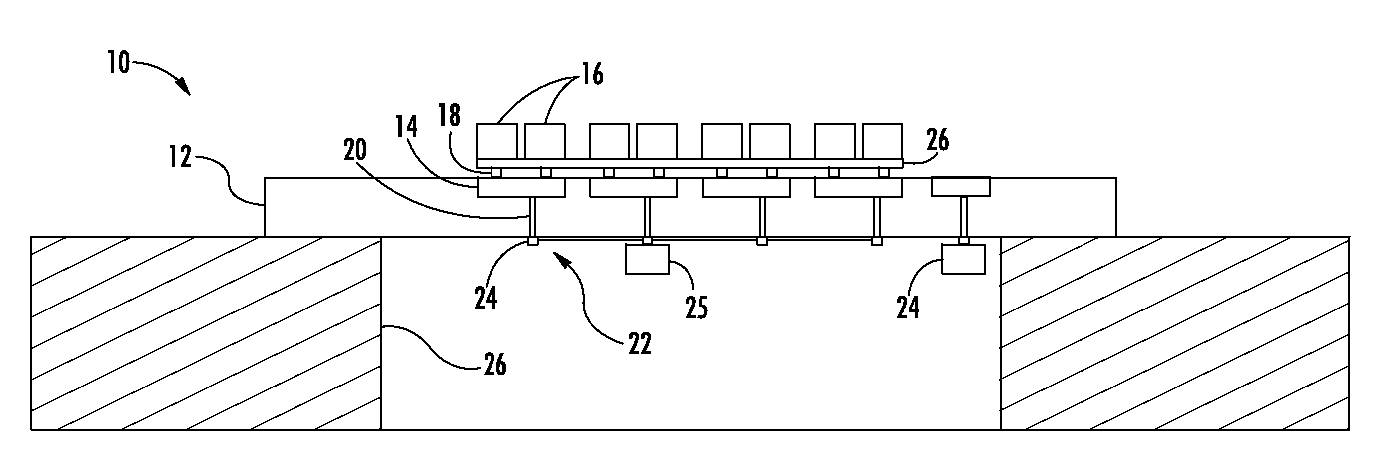
[0018]Referring initially to FIG. 1, a phased array antenna module 10 and a method of making the phased array antenna module is now described. The phased array antenna module 10 includes a semiconductor wafer (or wafer tile) 12, such as may be fabricated from a silicon germanium (SiGe) in a bipolar complementary metal-oxide-semiconductor (BiCMOS) process, although it should be appreciated that wafers fabricated in other semiconductor processes may be used....


PUM


Abstract

A phased array antenna includes a semiconductor wafer, with radio frequency (RF) circuitry fabricated on top side of the semiconductor wafer. There is an array of antenna elements above the top side of the semiconductor wafer, and a coaxial coupling arrangement coupling the RF circuitry and the array of antenna elements. The coaxial coupling arrangement may include a plurality of coaxial connections, each having an outer conductor, an inner conductor, and a dielectric material therebetween. The dielectric material may be air.

Description

FIELD OF THE INVENTION[0001]The present invention relates to the field of antenna modules, and, more particularly, to phased array antenna modules and related methods.BACKGROUND OF THE INVENTION[0002]A phased array antenna comprises a group of antenna elements in which the relative phases of the respective signals feeding the antenna elements are varied thereby controlling the radiation pattern of the phased array antenna. The interface between the feed network and the antenna elements typically comprises connectors and cabling, and the connectors typically used may suffer from high signal loss. The connectors used for the interface may also be expensive and some antennas may require multiple connectors for each antenna element thereby adding complexity and / or cost to the antenna. In addition, space limitations on the antenna may result in size limitations on the connectors and / or make the removal of heat difficult.[0003]U.S. Pat. No. 5,327,152 to Kruger et al. discloses an active a...

Claims


Application Information

Patent Timeline
Patent Type & Authority Applications(United States)
IPC IPC(8): H01Q21/00H01L21/77
CPCH01P3/06H01Q21/0093H01Q21/0025H01Q21/0006
Inventor PARADISO, LOUIS R.ORTIZ, SEANHEGE, DONALD FRANKLINRAWNICK, JAMES J.THEISS, LORA A.SCHAPPACHER, JERRY B.
Owner HARRIS CORP
Learn More