Semiconductor process

a technology of semiconductors and processes, applied in the field of semiconductor processes, can solve the problems of insufficient stress forcing of gate channels, difficult removal of spacers, limited ability to enhance carrier mobility of gate channels through epitaxial layers, etc., and achieve the effect of improving the performance of semiconductor structures, facilitating stress removal, and facilitating stress removal

Active Publication Date: 2013-02-28
UNITED MICROELECTRONICS CORP
View PDF7 Cites 39 Cited by
  • Summary
  • Abstract
  • Description
  • Claims
  • Application Information

AI Technical Summary

Benefits of technology

[0010]The present invention provides a semiconductor process, that etches at least a recess having a specific profile structure in the fin-shaped structure beside the gate structure. Thus, an epitaxial layer having a hexagon-shaped profile structure can be formed in the recess, and the performance of the semiconductor structure can therefore be improved. For example, the epitaxial layer formed in the present invention can make spacers easier to be removed. Besides, the epitaxial layer formed in the present invention can be easier to force stresses to the gate channel below the gate structure, so that improving the carrier mobility in the gate channel.

Problems solved by technology

However, the epitaxial layers make removal of the spacers difficult.
The distance between the epitaxial layers on either side of the gate structure is also too great, resulting in insufficient stress forcing the gate channel below the gate structure, and limited ability to enhance carrier mobility of the gate channel through the epitaxial layers.

Method used


Image

  • Semiconductor process
  • Semiconductor process
  • Semiconductor process

Examples


Embodiment Construction

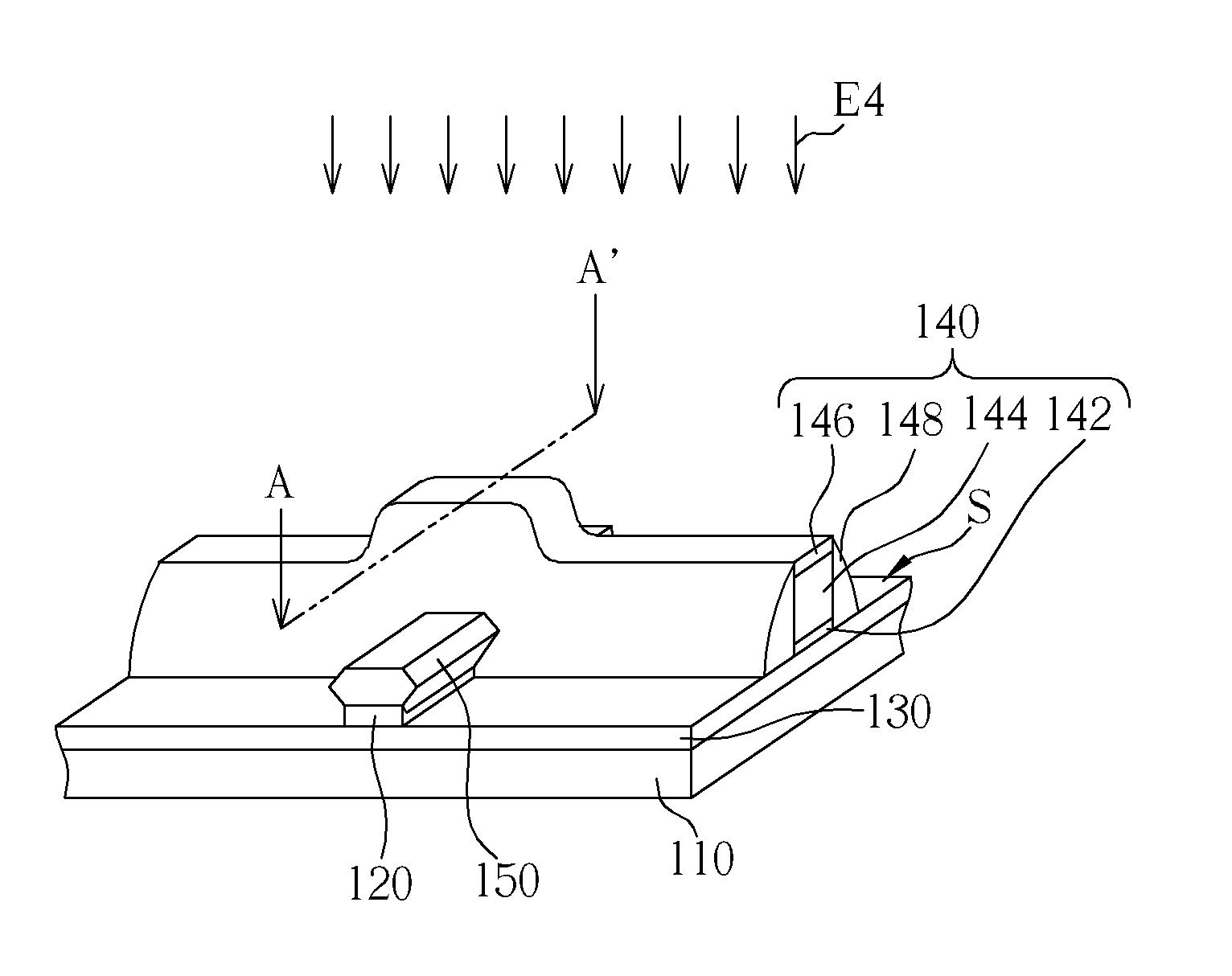
[0015]FIGS. 1-8 schematically depict a stereo view of a semiconductor process according to one preferred embodiment of the present invention. FIG. 9 schematically depicts a cross-sectional view of a semiconductor process along line A-A′ and above the plane S of FIG. 7. FIG. 10 schematically depicts a cross-sectional view of a semiconductor process along line A-A′ and above the plane S of FIG. 8. The semiconductor process of the present invention is suited for application to a bulk substrate or a silicon-on-insulator substrate.

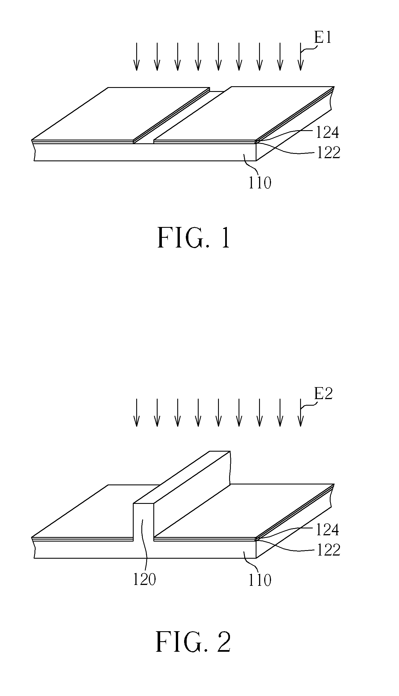
[0016]Please refer to FIGS. 1-3. As shown in FIG. 1, a substrate 110 is provided, wherein the substrate 110 is a bulk substrate, for example. A mask layer (not shown) is formed on the substrate, wherein the mask layer includes a pad oxide layer (not shown) and a nitride layer (not shown) located on the pad oxide layer. A photolithography process E1 is performed to pattern the mask layer for forming a patterned pad oxide layer 122 and a patterned nitride layer 1...


PUM


Abstract

A semiconductor process includes the following steps. A substrate is provided. At least a fin-shaped structure is formed on the substrate. An oxide layer is formed on the substrate without the fin-shaped structure being formed thereon. A gate is formed to cover a part of the oxide layer and a part of the fin-shaped structure. An etching process is performed to etch a part of the fin-shaped structure beside the gate, therefore at least a recess is formed in the fin-shaped structure. An epitaxial process is performed to form an epitaxial layer in the recess, wherein the epitaxial layer has a hexagon-shaped profile structure.

Description

BACKGROUND OF THE INVENTION[0001]1. Field of the Invention[0002]The present invention relates generally to a semiconductor process, and more specifically, to a semiconductor process that forms at least a recess in a fin-shaped structure beside a gate structure, thereby forming an epitaxial layer having a hexagon-shaped profile structure in the recess.[0003]2. Description of the Prior Art[0004]With increasing miniaturization of semiconductor devices, various Fin-shaped field effect transistor (FinFET) devices have been developed. The Fin-shaped field effect transistor (FinFET) is advantageous for the following reasons. First, manufacturing processes of Fin-shaped field effect transistor (FinFET) devices can be integrated into traditional logic device processes, and thus are more compatible. In addition, since the three-dimensional structure of the FinFET increases the overlapping area between the gate and the substrate, the channel region is controlled more effectively. This therefor...

Claims


Application Information

Patent Timeline
Patent Type & Authority Applications(United States)
IPC IPC(8): H01L21/336
CPCH01L29/66795H01L29/66628
Inventor LIAO, CHIN-IHSU, CHIA-LINLI, MING-YENWU, HSIN-HUEIHSIEH, YUNG-LUNCHEN, CHIEN-HAOLEE, BO-SYUAN
Owner UNITED MICROELECTRONICS CORP
Why Eureka
Try Eureka