
Discrete Three-Dimensional Memory

a three-dimensional memory and disk technology, applied in the field of integrated circuits, can solve the problems of occupying a large die area, difficult design of peripheral circuits, and reducing the manufacturing cost of 3d-m, so as to improve performance, reduce cost, and improve the array efficiency of memory-array dies

Active Publication Date: 2013-03-07
CHENGDU HAICUN IP TECH +1
View PDF8 Cites 3 Cited by
  • Summary
  • Abstract
  • Description
  • Claims
  • Application Information

AI Technical Summary

Benefits of technology

The present invention aims to provide a 3D-M with improved performance and lower cost. The technical effects would therefore include better performance and more affordable access to 3D-M technology.

Problems solved by technology

Because the 3D-M arrays use a complex back-end process while their peripheral circuits use a relatively simple back-end process, integrating the 3D-M arrays with their peripheral circuits will force the peripheral circuits to use the expensive manufacturing process for the 3D-M arrays.
As a result, integration does not reduce the manufacturing cost of the 3D-M, but actually increases it.
In addition, because the peripheral circuits is constrained by the 3D-M arrays in the number of the substrate metal levels, the peripheral circuits are difficult to design and occupy a large die area.
These materials degrade the overall 3D-M performance.

Method used


Image

  • Discrete Three-Dimensional Memory
  • Discrete Three-Dimensional Memory
  • Discrete Three-Dimensional Memory

Examples


Embodiment Construction

[0027]Those of ordinary skills in the art will realize that the following description of the present invention is illustrative only and is not intended to be in any way limiting. Other embodiments of the invention will readily suggest themselves to such skilled persons from an examination of the within disclosure.

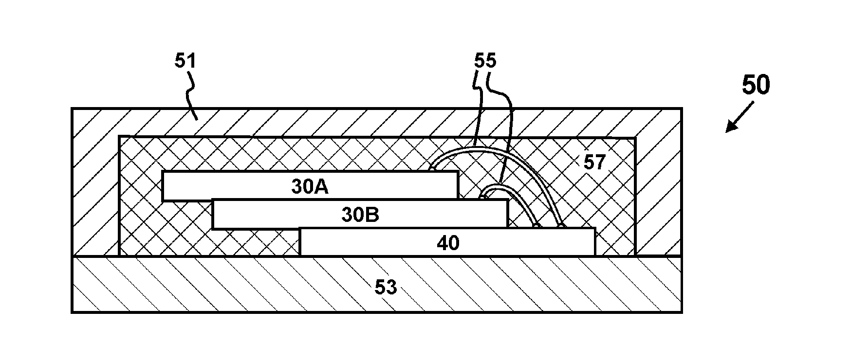
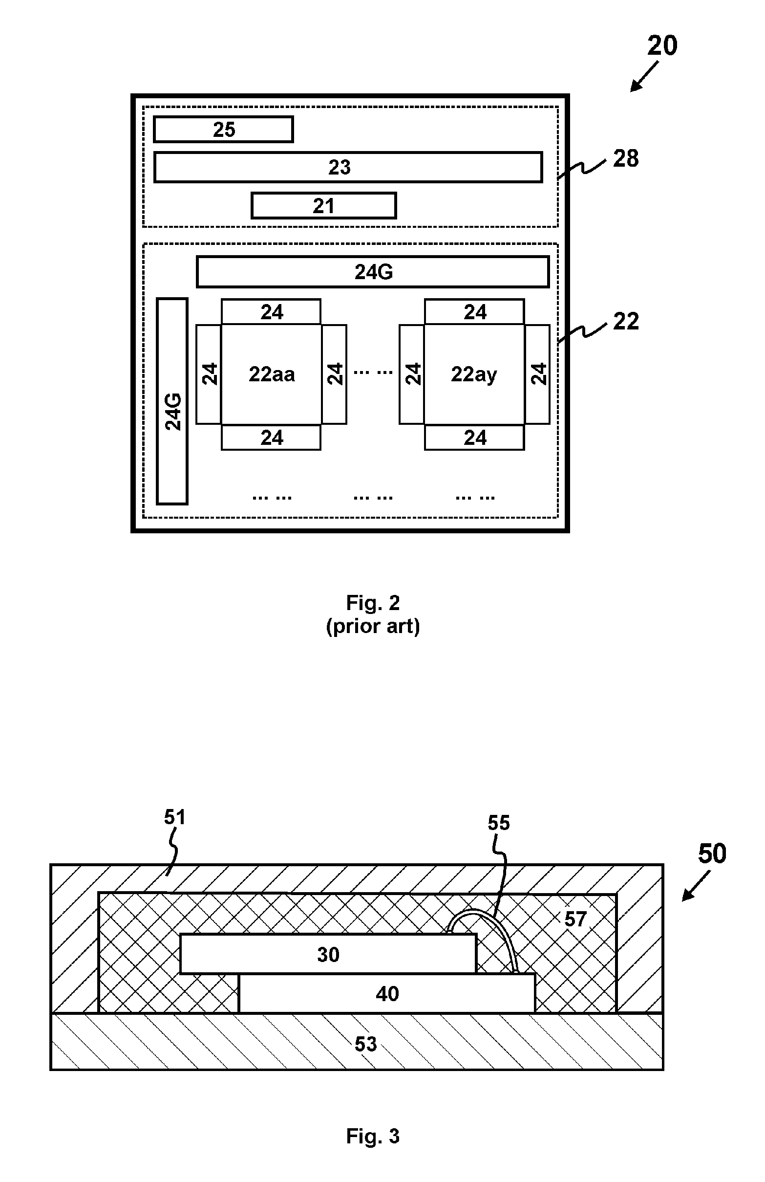
[0028]Referring now to FIG. 3, a preferred discrete 3D-M package 50 is disclosed. It comprises at least two discrete dice: a memory-array die 30 and a peripheral-circuit die 40. These dice 30, 40 are stacked on a package substrate 53 and located inside a package housing 51. Bond wires 55 provide electrical connection between the dice 30 and 40. Here, bond wire 55 is a coupling means between the memory-array die 30 and the peripheral-circuit die 40. Other coupling means include solder bump. To ensure data security, the dice 30, 40 are preferably encapsulated into a molding compound 57. In this preferred embodiment, the memory-array die 30 is vertically stacked above the peri...


PUM

PropertyMeasurementUnit
programming voltageaaaaaaaaaa
read voltageaaaaaaaaaa
temperatureaaaaaaaaaa

Abstract

The present invention discloses a discrete three-dimensional memory (3D-M). It is partitioned into at least two discrete dice: a memory-array die and a peripheral-circuit die. The memory-array die comprises at least a 3D-M array, which is built in a 3-D space. The peripheral-circuit die comprises at least a peripheral-circuit component, which is built on a 2-D plane. At least one peripheral-circuit component of the 3D-M is formed in the peripheral-circuit die instead of in the memory-array die. The array efficiency of the memory-array die can be larger than 70%.

Description

CROSS-REFERENCE TO RELATED APPLICATIONS[0001]This application relates to a provisional application, “Three-Dimensional Memory with Separate Memory-Array and Peripheral-Circuit Substrates”, Application Ser. No. 61 / 529,929, filed Sep. 1, 2011.BACKGROUND[0002]1. Technical Field of the Invention[0003]The present invention relates to the field of integrated circuit, and more particularly to three-dimensional memory (3D-M).[0004]2. Prior Arts[0005]Three-dimensional memory (3D-M) is a semiconductor memory comprising a plurality of vertically stacked memory levels. It includes three-dimensional read-only memory (3D-ROM) and three-dimensional random-access memory (3D-RAM). The 3D-ROM can be further categorized into three-dimensional mask-programmed read-only memory (3D-MPROM) and three-dimensional electrically-programmable read-only memory (3D-EPROM). Based on programming mechanism, 3D-M may be categorized into memristor, resistive random-access memory (RRAM or ReRAM), phase-change memory, p...

Claims


Application Information

Patent Timeline
Patent Type & Authority Applications(United States)
IPC IPC(8): H01L25/16
CPCH01L2225/06506H01L2225/06562H01L2225/107H01L25/0657H01L2225/1023H01L25/18H01L25/105H01L2224/48145H01L2224/48227H01L2224/73265G11C5/02H01L2224/32145H01L2224/32225H01L2924/00012H01L24/73
Inventor ZHANG, GUOBIAO
Owner CHENGDU HAICUN IP TECH
Learn More