

ESD protection circuit
- Summary
- Abstract
- Description
- Claims
- Application Information
AI Technical Summary
Benefits of technology
Problems solved by technology
Method used
Image

Examples
Embodiment Construction
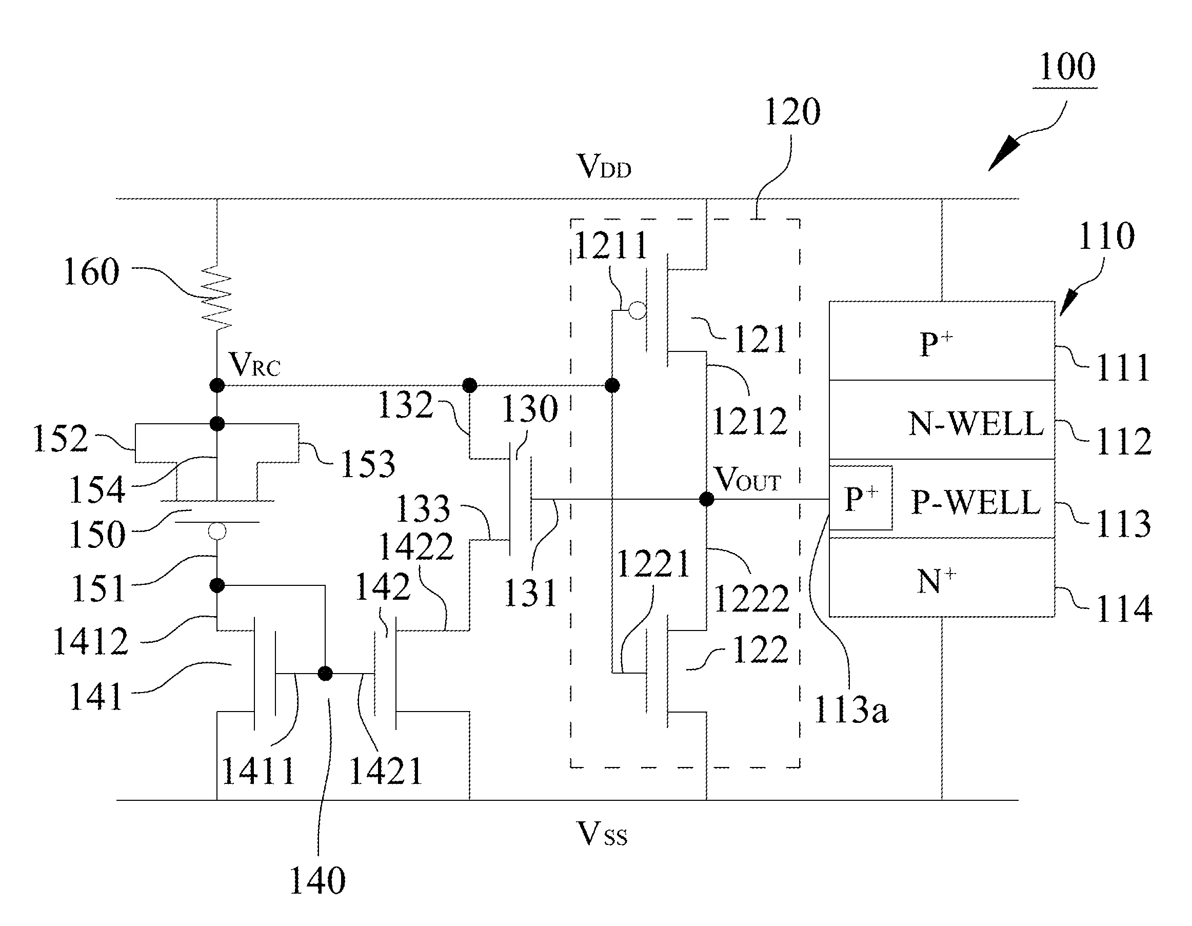
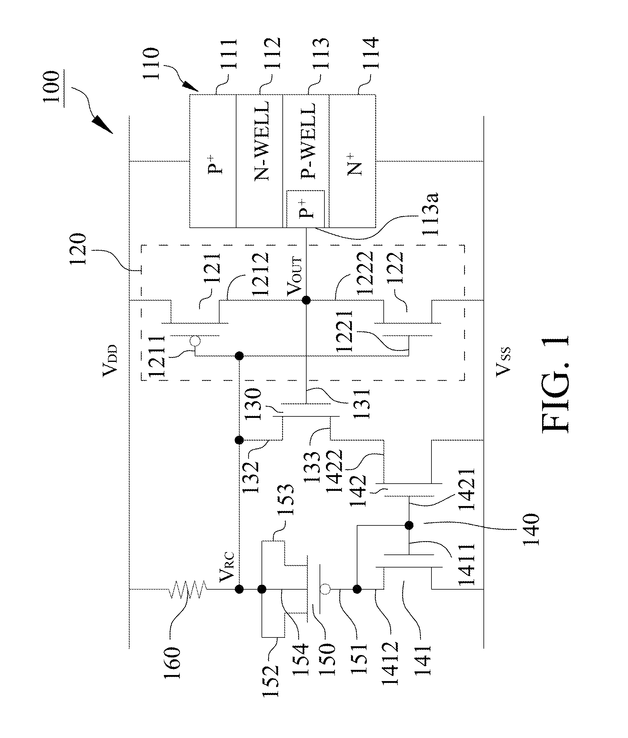
[0010]With reference to FIG. 1, an ESD protection circuit 100 in accordance with a first embodiment of the present invention includes a silicon controlled rectifier 110, a first CMOS inverter 120, a first transistor 130, a current mirror 140, a PMOS capacitor 150 and a resistor 160, wherein the first CMOS inverter 120 electrically connects with the silicon controlled rectifier 110. The first transistor 130 comprises a first end 131, a second end 132 and a third end 133, wherein the first end 131 electrically connects with the silicon controlled rectifier 110 and the first CMOS inverter 120, and the current mirror 140 electrically connects with the third end 133 of the first transistor 130. The PMOS capacitor 150 comprises a fourth end 151, a fifth end 152 and a sixth end 153, the fourth end 151 of the PMOS capacitor 150 electrically connects with the current mirror 140, and the resistor 160 electrically connects with the first CMOS inverter 120, the second end 132 of the first trans...
PUM
 Abstract
Description
Claims
Application Information