Film deposition apparatus, film deposition method and storage medium

a film deposition apparatus and film deposition technology, applied in chemical vapor deposition coatings, electric discharge tubes, coatings, etc., can solve the problems of not implementing a sufficient plasma process, affecting the effect of plasma, and causing electric damage to the interconnection structure of plasma,

Active Publication Date: 2013-03-07
TOKYO ELECTRON LTD
View PDF6 Cites 149 Cited by
  • Summary
  • Abstract
  • Description
  • Claims
  • Application Information

AI Technical Summary

Benefits of technology

[0010]Embodiments of the present invention provide a novel and useful film deposition apparatus

Problems solved by technology

At this time, if an interconnection structure is formed inside a wafer, there is a concern that the plasma gives electric damage to the interconnection structure.
On the other hand, if a plasma source is away from the wafer to reduce the plasma damage to the wafer, because an activated species such as ions and radicals in the plasma readily become inactivated under a pressure condition of performing the film deposition process, there is a concern that it becomes difficult for the activated species to reach the wafer and a sufficient plasma

Method used


Image

  • Film deposition apparatus, film deposition method and storage medium
  • Film deposition apparatus, film deposition method and storage medium
  • Film deposition apparatus, film deposition method and storage medium

Examples


Embodiment Construction

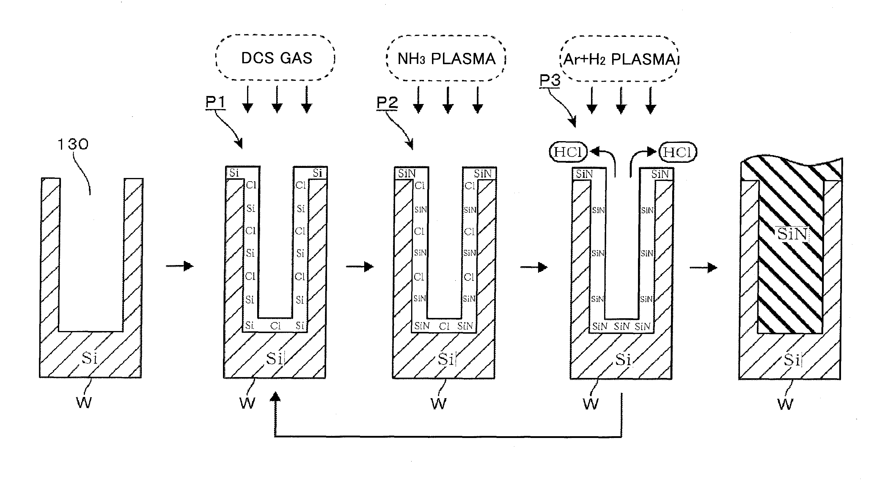
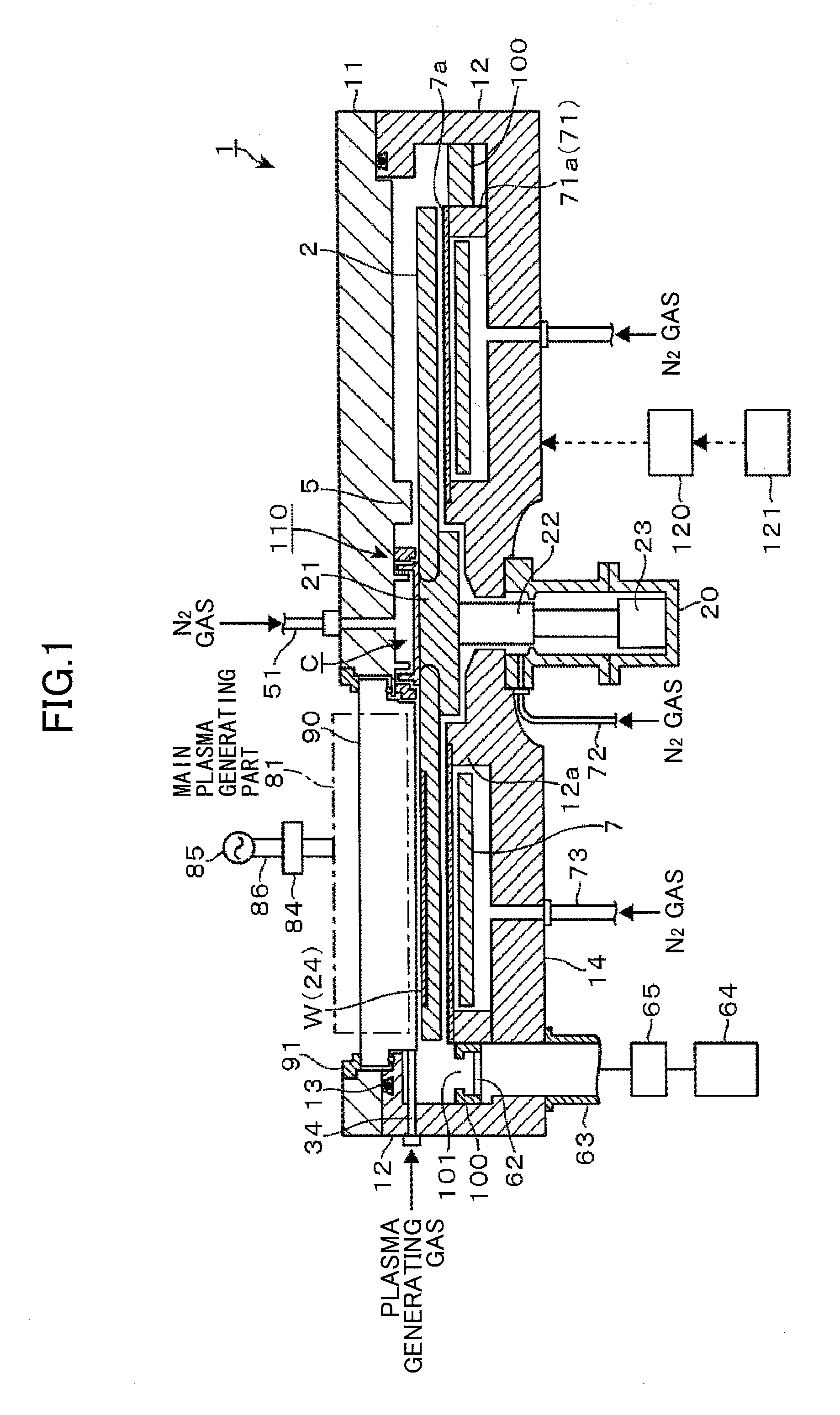
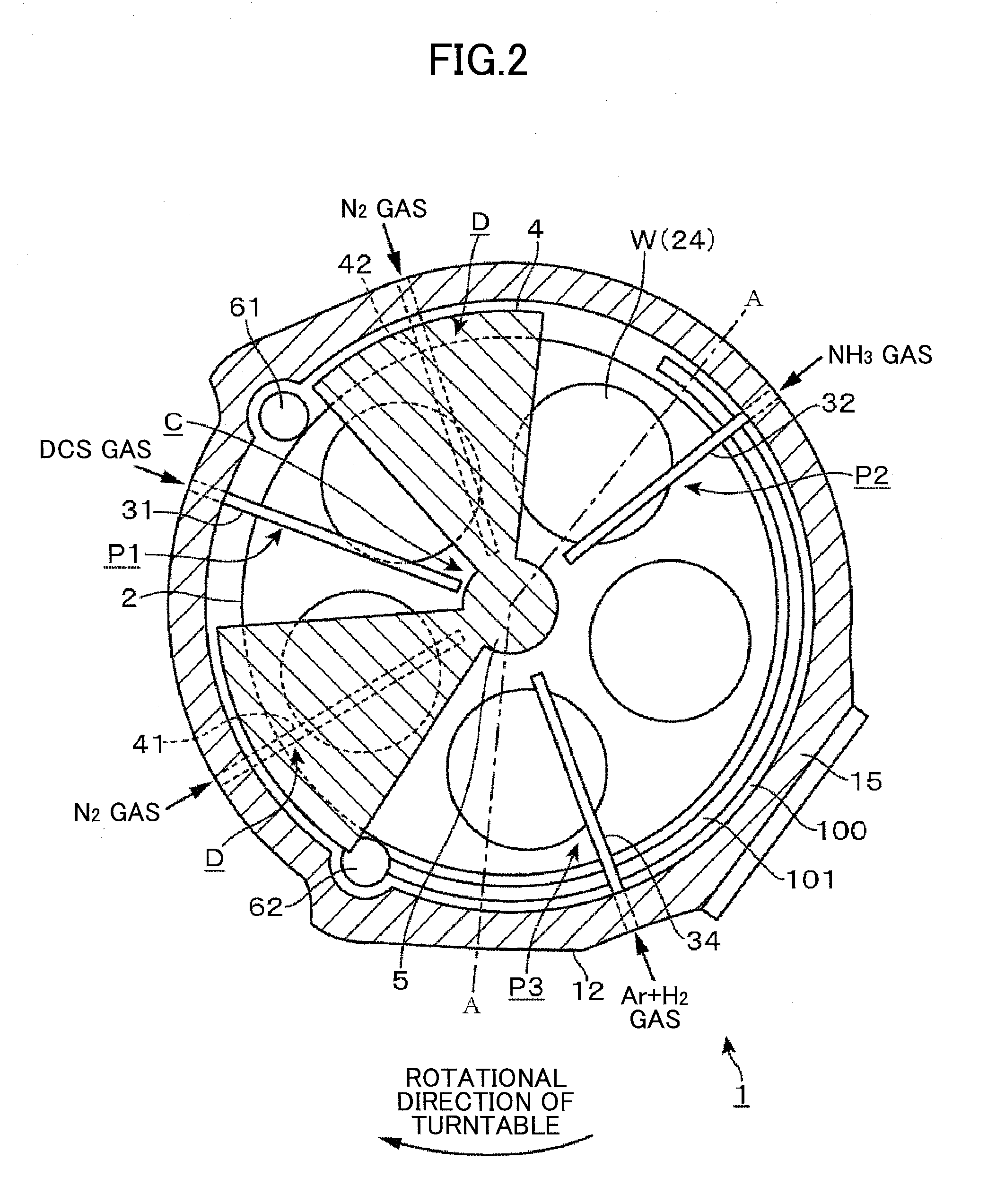
[0042]A description is given below, with reference to drawings of embodiments of the present invention. More specifically, a description is given about an example of a film deposition apparatus of an embodiment with reference to FIGS. 1 through 11. As shown in FIGS. 1 and 2, this film deposition apparatus includes a vacuum chamber 1 whose planar shape is an approximately round shape, and a turntable 2 provided in the vacuum chamber 1 and having the rotation center that coincides with the center of the vacuum chamber 1. As described below in detail, the film deposition apparatus is configured to deposit a thin film by laminating a reaction product on a surface of a wafer W by an ALD method, and configured to perform a plasma process onto the wafer W in the middle of depositing the thin film. At this time, in performing the plasma process, the film deposition apparatus is configured to not give electrical damage to the wafer by the plasma, or to reduce the electrical damage as much as...


PUM

PropertyMeasurementUnit
Dielectric polarization enthalpyaaaaaaaaaa
Sizeaaaaaaaaaa
Electric fieldaaaaaaaaaa

Abstract

A film deposition apparatus includes a turntable having a substrate mounting area, a first plasma gas supplying part, a second plasma supplying part, a first plasma gas generating part to convert the first plasma generating gas to first plasma, and a second plasma generating part provided away from the first plasma generating part in a circumferential direction and to convert the second plasma generating gas to second plasma. The first plasma generating part includes an antenna facing the turntable so as to convert the first plasma generating gas to the first plasma, and a grounded Faraday shield between the antenna and an area where a plasma process is performed, and to include plural slits respectively extending in directions perpendicular to the antenna and arranged along an antenna extending direction to prevent an electric field from passing toward the substrate and to pass a magnetic field toward the substrate.

Description

CROSS-REFERENCE TO RELATED APPLICATIONS[0001]This patent application is based upon and claims the benefit of priority of Japanese Patent Application No. 2011-193046, filed on Sep. 5, 2011, the entire contents of which are incorporated herein by reference.BACKGROUND OF THE INVENTION[0002]1. Field of the Invention[0003]The present invention relates to a film deposition apparatus, a film deposition method and a storage medium that deposit a reaction product on a surface of a substrate in a layer-by layer manner by supplying process gases that react to each other and perform a plasma process onto the substrate.[0004]2. Description of the Related Art[0005]An ALD (Atomic Layer Deposition) method that deposits a reaction product of plural kinds of process gases (i.e., reaction gases) that react to each other in a layer-by-layer manner on a surface of a substrate such as a semiconductor wafer (which is called a “wafer” hereinafter) by supplying the plural kinds of process gases in turn is t...

Claims


Application Information

Patent Timeline
IPC IPC(8): C23C16/505H01L21/50
CPCC23C16/345C23C16/45551C23C16/45542H01L21/205H01J37/321H01J37/32733
Inventor KATO, HITOSHIHISHIYA, KATSUYUKIUSHIKUBO, SHIGEHIRO
Owner TOKYO ELECTRON LTD
Why Eureka
Try Eureka