Multi-spectrum photosensitive device

a multi-spectrum, photosensitive technology, applied in the direction of photometry using electric radiation detectors, optical radiation measurement, instruments, etc., can solve the problems of difficult manufacturing of three-layer sensing technology, complicated, and inability to industrialize very well, so as to improve the flexibility, the effect of easy color light sensing and better color sensing performan

Active Publication Date: 2013-03-14
BOLY MEDIA COMM SHENZHEN
View PDF13 Cites 44 Cited by
  • Summary
  • Abstract
  • Description
  • Claims
  • Application Information

AI Technical Summary

Benefits of technology

[0030]The beneficial technical effects of the present disclosure are designed to:
[0031]1. A better color sensing performance is provided and a color sensing device is integrated with an infrared sensing device. In the present disclosure, at least two sensing pixel layers are provided in a direction of the light source irradiation in the form of composite sensing pixel containing at least two basic sensing pixels, the basic sensing pixels senses each spectral band of the spectrum at various layers, so that it is implemented that at least two spectral bands can be sensed at the same pixel position of one surface of the base layer but at different depths, so as to provide a better flexibility and a more pixel disposition on pattern arrangement of composite sensing pixel macro unit of the surface thereon, so that the sensibility, resolution and dynamic scope of the sensing device are greatly enhanced. On the other hand, when two sensing pixel layers are disposed as one sensing visible light and the other sensing infrared light, the integration of visible light device and infrared light device is realizable easily to sense color light and infrared light simultaneously.
[0032]2. The processing technique implementing products is simple. By adopting existing CCD or CMOS sensing chip processing techniques and equipment, the present disclosure could easily manufacture a single-sided double-layer multi-spectrum sensing device, double-sided double-layer multi-spectrum sensing device and double-sided multi-spectrum sensing device for front side sensing, back side sensing or double-direction sensing. For the Foveon company's three-layer sensing device mentioned above, in order to carry out color sensing, it is necessary to dispose three layers at the same position to respectively sense three RGB colors so as to carry out color reconstruction. However, such method is difficult in processing three layers, and obviously makes wiring between transistors difficult, since connectors for different layers need to be separated from each other. Based on that, it is almost impossible for adding one more layer to the three RGB layers to perform infrared sensing. While the present disclosure carries out color reconstruction with p

Problems solved by technology

There are three main reasons for failure of the existing sensing device in integrating the color sensing device with infrared sensing device.
Though this method does not use the filter film, the manufacture of the three-layer sensing technology has been very difficult and industrialization is not very successful.
If an infrared layer is further added below the three layers, it will be more complicated

Method used


Image

  • Multi-spectrum photosensitive device
  • Multi-spectrum photosensitive device
  • Multi-spectrum photosensitive device

Examples


Embodiment Construction

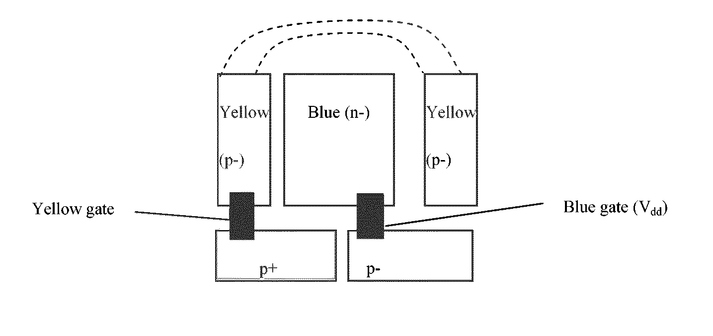
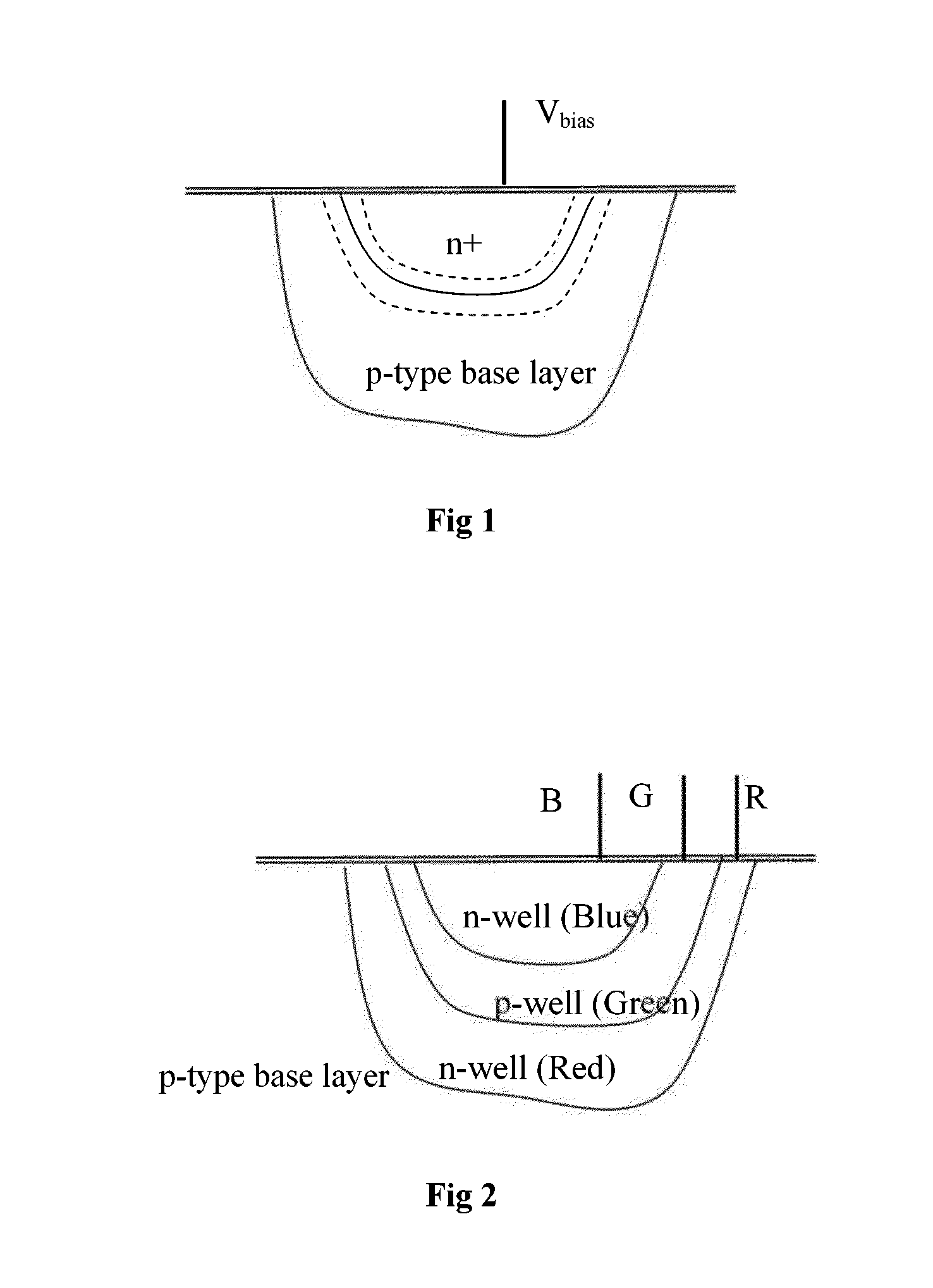
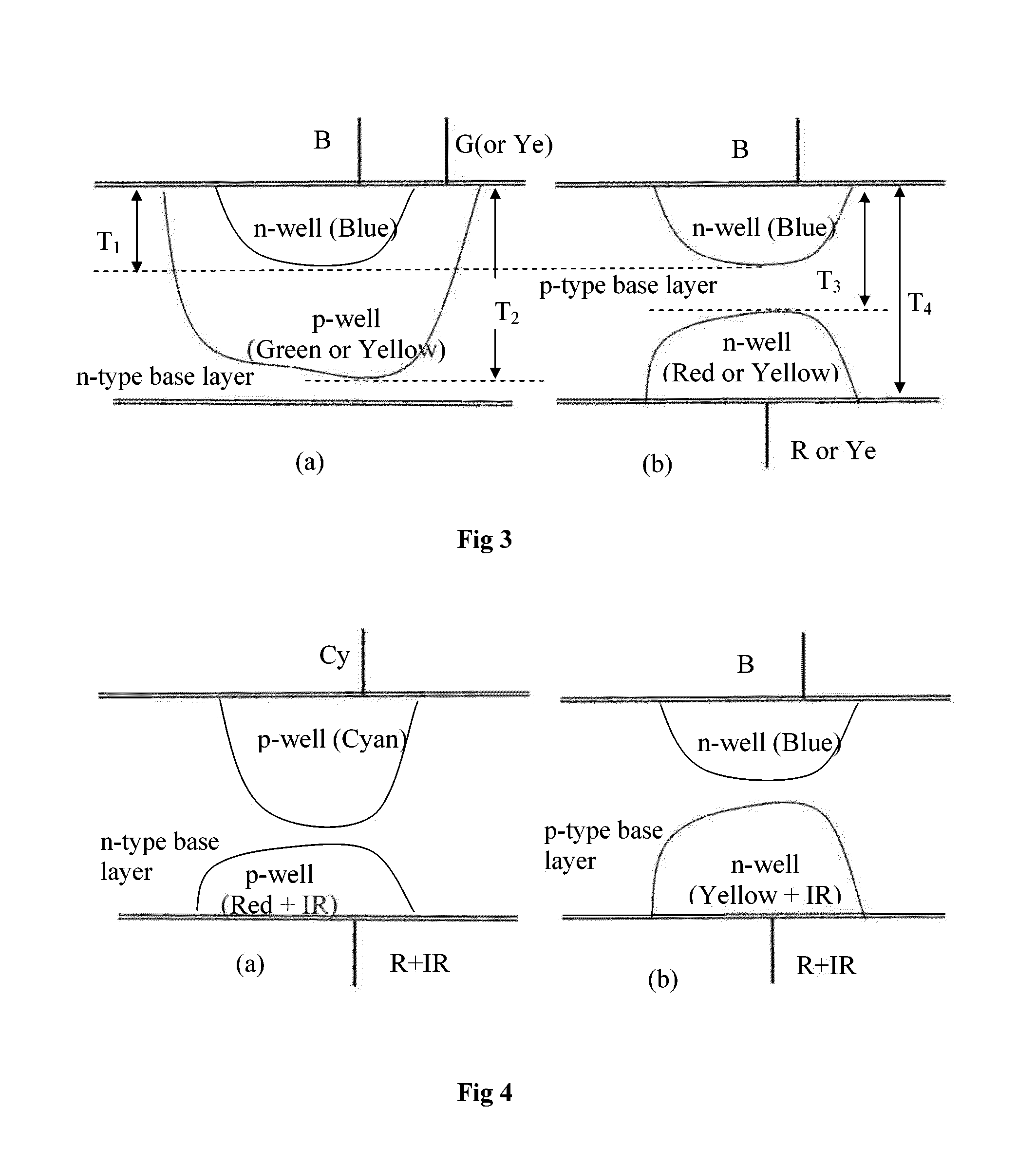
[0065]In order to facilitate describing the disclosure and explaining differences between the invention and existing technology, the following definition of the terms are provided: double-layer sensing device, multi-layer sensing device, double-sided sensing device, double-direction sensing device. The double-layer sensing device means that sensing pixels thereof are physically divided into two layers, each of which contains sensing pixels for sensing specific spectrum. The multi-layer sensing device refers to a sensing device with more than two layers, such as Foveon Company's X3 sensing device. The double-sided sensing device refers to a sensing device with two sensing surfaces, each of which can sense light from at least one direction. The bidirectional sensing device means that the sensing device can sense light from two directions (which usually form an angle of 180 degrees), i.e., both the front side and the back side of the sensing device can sense light.

[0066]A sensing devic...


PUM


Abstract

A multi-spectrum photosensitive device comprises two, three, or four composite sensing pixels arranged in layers up and down in a base layer of P-type or N-type silicon by means of single-sided processing or double-sided processing, each composite sensing pixels can sense respectively spectrum orthogonal or complementary to each other in visible light or visible and infrared light. The basic sensing pixels on different layers of the composite sensing pixels can be designed to sense different colors or spectrums, so that a multi-spectrum photosensitive chip can be achieved by repeatedly arranging the macro units consisting of more than one composite sensing pixel. The present disclosure also includes a new multi-layer sensing pixel, and examples of which used in a single-sided double-layer, or a double-sided double-layer, or a double-sided three-layer, or a double-sided four-layer, or a single-sided mixed double-layer, or a double-sided mixed with double-layer or a multi-layer multi-spectrum sensing device. A multi-spectrum photosensitive device according to the present disclosure has the advantage of better color sensing performance, integration of color sensing and infrared sensing, and a simple processing technique.

Description

TECHNICAL FIELD[0001]The present disclosure relates to a multi-spectrum photosensitive device, in particular, to physical implementation and manufacture thereof. More particularly, the present invention relates to a sensing device for panchromatic images which is achievable by CCD or CMOS semiconductor for simultaneously sensing several spectra (such as visible light and infrared). Herein, the panchromatic spectrum (or color) comprises the entire spectra of interest. For normal sensing devices (e.g., those for visible light), the panchromatic refers to the entire spectra of visible light that contains red, green, blue and white. For sensing devices used for a combination of infrared and visible light, the panchromatic refers to spectra of the visible light and infrared. The present disclosure applies to multi-spectrum sensing device for sensing infrared, monochrome and color images.BACKGROUND ART[0002]The present disclosure is a continuation of earlier applications titled “Multi-spe...

Claims


Application Information

Patent Timeline
IPC IPC(8): G01J1/42
CPCH01L27/14647H01L31/0352H01L27/14652H01L27/14641H01L27/1464G01N21/6452H01L27/14649G01J1/42G01N21/6454H04N25/17H01L27/14
Inventor HU, XIAOPING
Owner BOLY MEDIA COMM SHENZHEN
Why Eureka
Try Eureka