
Eureka
For R&D, Eureka makes reading and utilizing patents & technical documents easy.
Eureka AIR
Designed for self-driven R&D workflows. Generate viable solutions, solve complex R&D challenges, empower your innovation with AI.

Eureka Materials
Designed for material experts only. Revolutionize your material R&D, from search, analyze, to developing new materials.

TechResearch
Generate reliable direction feasibility study reports for your R&D in just a few steps.

TechSeek
Discover and master advanced knowledge NOW. Basics, ideas, possibilities, all at once.

TechMind
As an expert in R&D Theories, TechMind can generates customized viable solutions instantly.

TechRisk
Analyze your overall solution with one click, know your potential R&D risks in advance.

TechMonitor
Get weekly tech updates, stay abreast of the latest tech innovations and key insights.
Electrical test structure applying 3d-ics bonding technology for stacking error measurement
- Summary
- Abstract
- Description
- Claims
- Application Information
AI Technical Summary
Benefits of technology
Problems solved by technology
Method used
Image

Examples
Embodiment Construction
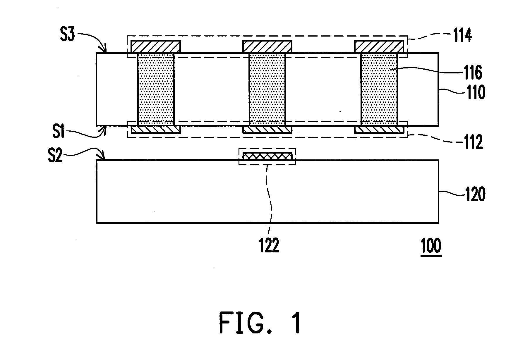
[0037]When an integrated circuit is measured, how to measure an internal circuit of the integrated circuit from a surface of the integrated circuit is a first problem encountered. In a conventional technique, a through-silicon via (TSV) technique is generally used for electrical connection. The TSV technique is used to drill vias for electrical connection, and metal pads are disposed on the surface of the wafer for measurement.
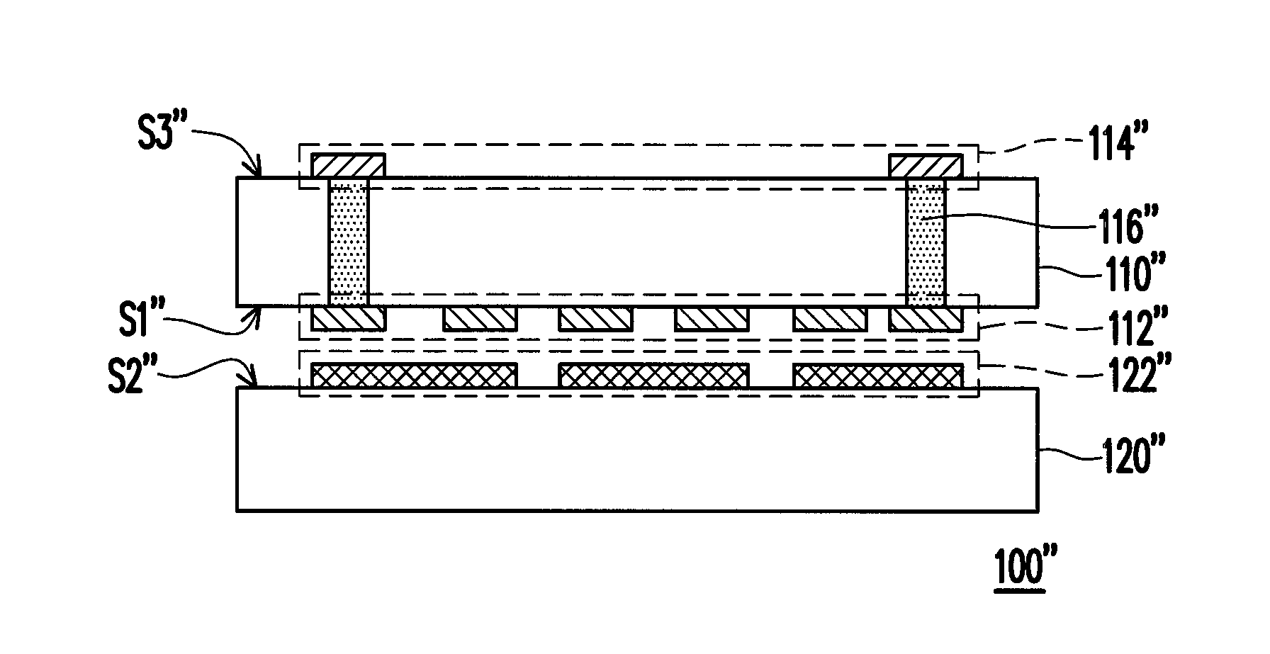
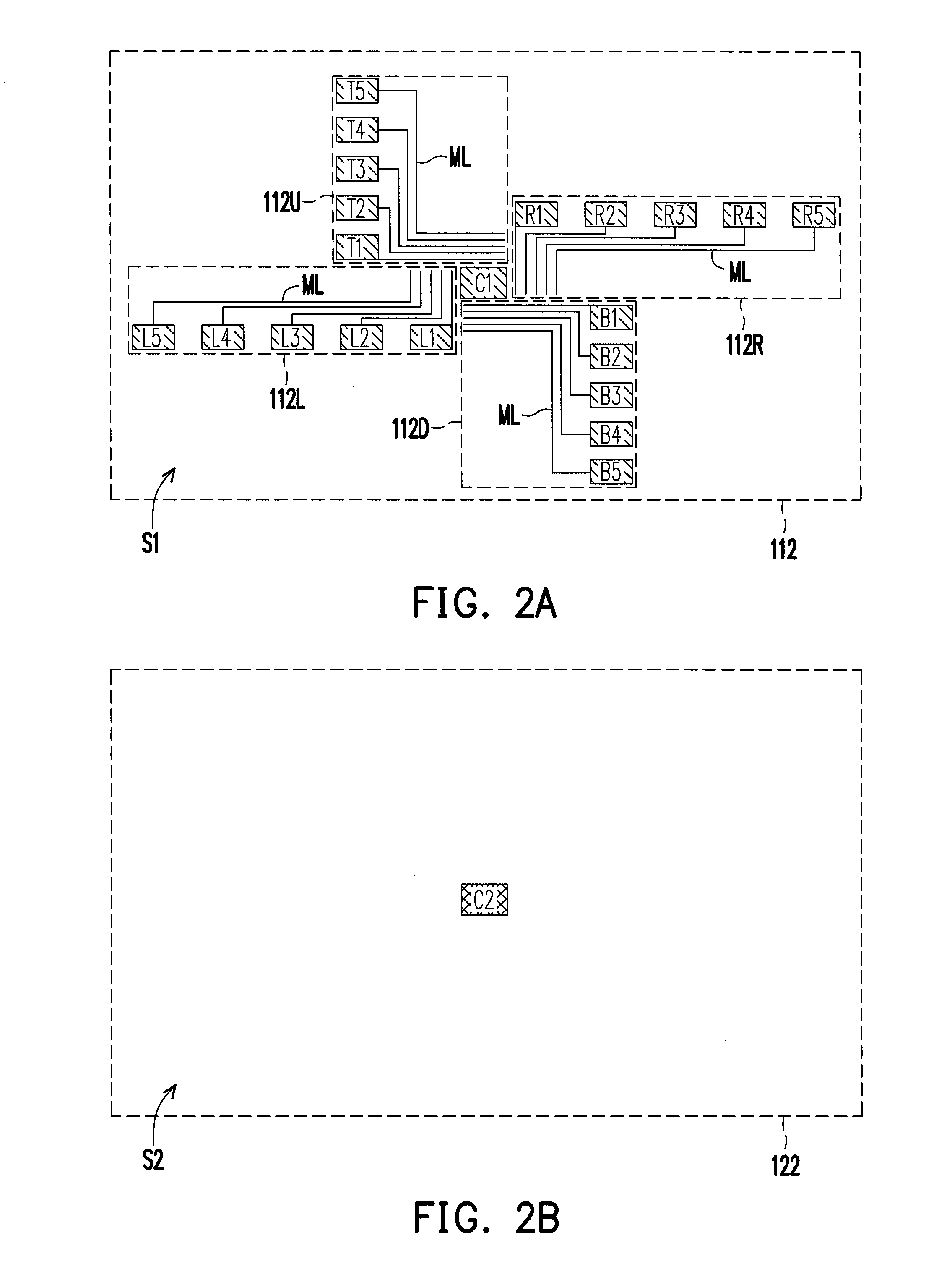
[0038]FIG. 1 is a schematic diagram of a three-dimensional (3D) integrated circuit 100 according to an embodiment of the invention. Referring to FIG. 1, the 3D integrated circuit 100 of the present embodiment includes a first wafer 110 and a second wafer 120, where the first wafer 110 is stacked on the second wafer 120. In the present embodiment, the first wafer 110 includes a first conductive pattern 112 and a third conductive pattern 114, which are respectively disposed on surfaces S1 and S3 of the first wafer 110. The second wafer 120 includes a second cond...
PUM
 Abstract
Description
Claims
Application Information
 - R&D Engineer
- R&D Manager
- IP Professional
- Industry Leading Data Capabilities
- Powerful AI technology
- Patent DNA Extraction
Browse by: Latest US Patents, China's latest patents, Technical Efficacy Thesaurus, Application Domain, Technology Topic, Popular Technical Reports.
© 2024 PatSnap. All rights reserved.Legal|Privacy policy|Modern Slavery Act Transparency Statement|Sitemap|About US| Contact US: help@patsnap.com