
Light-emitting device

Active Publication Date: 2013-03-14
SEMICON ENERGY LAB CO LTD
View PDF5 Cites 47 Cited by
  • Summary
  • Abstract
  • Description
  • Claims
  • Application Information

AI Technical Summary

Benefits of technology

The invention provides a light-emitting device that can reduce variations in brightness among pixels caused by differences in threshold voltage. By acquiring the threshold voltage and correcting it, this device can ensure consistent and uniform brightness across the entire display.

Problems solved by technology

Consequently, when the TFT 6 is normally on, the threshold voltage cannot be acquired, and generation of unevenness in luminance of a light-emitting element due to variations in threshold voltage cannot be prevented.

Method used


Image

  • Light-emitting device
  • Light-emitting device
  • Light-emitting device

Examples


embodiment 1

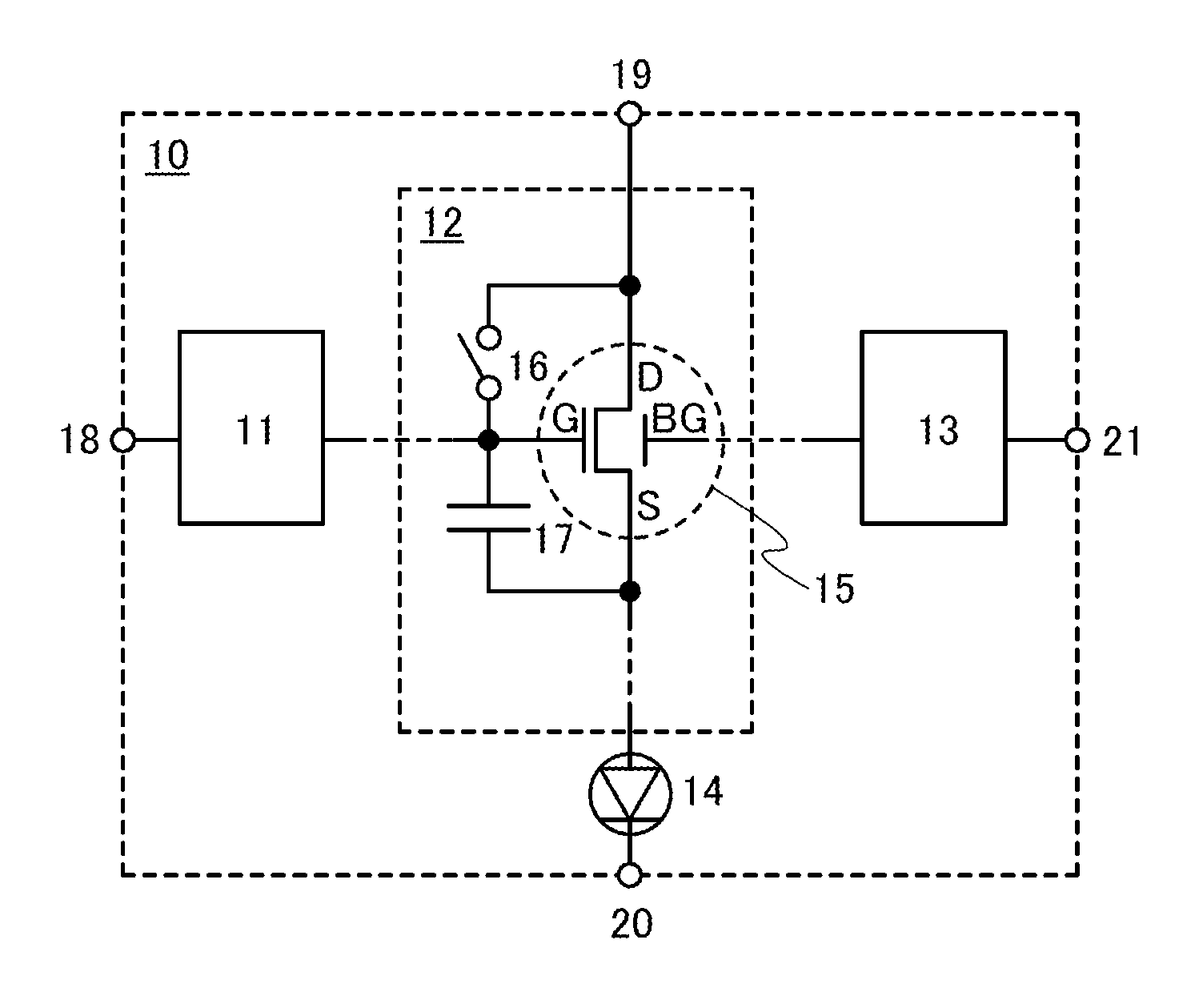
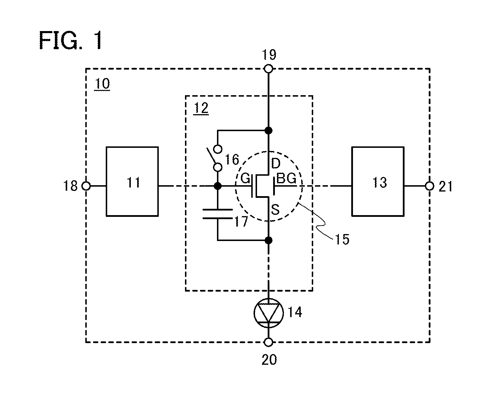
[0033]FIG. 1 illustrates the structure of a pixel included in a light-emitting device according to one embodiment of the present invention. A pixel 10 in FIG. 1 includes a switch 11, a circuit 12 for controlling the amount of current in response to an image signal, a switch 13, and a light-emitting element 14 supplied with the current from the circuit 12.

[0034]Specifically, the switch 11 controls whether an image signal supplied to a terminal 18 is supplied to the circuit 12. For example, the switch 11 can be one or more transistors. Alternatively, the switch 11 may be a capacitor instead of one or more transistors.

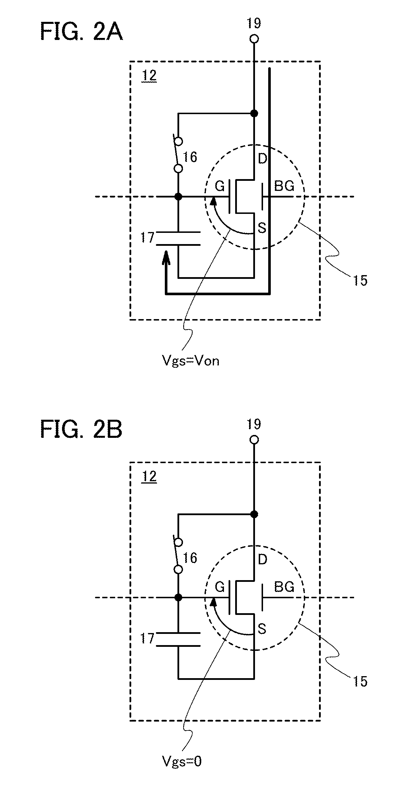
[0035]The circuit 12 includes a transistor 15 whose drain current is supplied to the light-emitting element 14, a switch 16, and a capacitor 17. The switch 16 selects conduction or non-conduction between a gate electrode (represented by G) and a drain terminal (represented by D) of the transistor 15, that is, controls connection between the gate electrode and the drain te...

embodiment 2

[0057]FIG. 4 illustrates a specific structure example of a pixel in a light-emitting device according to one embodiment of the present invention.

[0058]As in FIG. 1, the pixel 10 in FIG. 4 includes the switch 11, the circuit 12, the switch 13, and the light-emitting element 14. In the pixel 10 in FIG. 4, the switch 11 is a transistor 30. Further, the circuit 12 includes the transistor 15, the capacitor 17, transistors 31 to 36, and a capacitor 38. The transistor 31 corresponds to the switch 16 in FIG. 1. The switch 13 is a transistor 37.

[0059]Note that in FIG. 4, the transistor 15 is an n-channel transistor.

[0060]Specifically, in the pixel 10 in FIG. 4, a gate electrode of the transistor 30 is connected to a scan line GLa. One of a source terminal and a drain terminal of the transistor 30 is connected to the signal line SL. The other of the source terminal and the drain terminal of the transistor 30 is connected to the gate electrode of the transistor 15. A gate electrode of the tran...

embodiment 3

[0096]FIG. 10 illustrates a specific structure example of a pixel in a light-emitting device according to one embodiment of the present invention.

[0097]As in FIG. 1, the pixel 10 in FIG. 10 includes the switch 11, the circuit 12, the switch 13, and the light-emitting element 14. In the pixel 10 in FIG. 10, the switch 11 is a transistor 51. Further, the circuit 12 includes the transistor 15, the capacitor 17, transistors 52 to 55, and capacitors 57 and 58. The transistor 52 corresponds to the switch 16 in FIG. 1. The switch 13 is a transistor 56.

[0098]Note that in FIG. 10, the transistor 15 is an n-channel transistor.

[0099]Specifically, in the pixel 10 in FIG. 10, a gate electrode of the transistor 51 is connected to the scan line GLa. One of a source terminal and a drain terminal of the transistor 51 is connected to the signal line SL. The other of the source terminal and the drain terminal of the transistor 51 is connected to the gate electrode of the transistor 15 and one electrod...


PUM


Abstract

In a light-emitting device, supply of current is controlled using a transistor having a normal gate electrode (a first gate electrode) and a second gate electrode for controlling threshold voltage. The light-emitting device comprises one or more switches for selecting conduction or non-conduction between the first gate electrode and a drain terminal of the transistor. When the threshold voltage of the transistor is acquired, the first gate electrode and the drain terminal of the transistor are brought into conduction with the switch, and the threshold voltage of the transistor is shifted by controlling the potential of the second gate electrode.

Description

BACKGROUND OF THE INVENTION[0001]1. Field of the Invention[0002]The present invention relates to a light-emitting device in which a transistor is provided in each pixel.[0003]2. Description of the Related Art[0004]In an active matrix light-emitting device including light-emitting elements, in general, at least a light-emitting element, a transistor (a switching transistor) that controls input of image signals to pixels, and a transistor (a driving transistor) that controls the value of current supplied to the light-emitting element in response to an image signal are provided in each pixel. In a light-emitting device having the above structure, drain current of a driving transistor is supplied to a light-emitting element; thus, when the threshold voltage of driving transistors varies among pixels, the luminance of light-emitting elements varies correspondingly.[0005]Patent Document 1 discloses a display device in which the threshold voltage of a TFT 6 (a driver element) is corrected ...

Claims


Application Information

Patent Timeline
IPC IPC(8): G09G5/00H05B44/00
CPCG09G3/32G09G3/3233G09G2300/0819G09G2320/0233G09G2300/0861G09G2310/0262G09G2300/0852H10K59/1213
Inventor MIYAKE, HIROYUKI
Owner SEMICON ENERGY LAB CO LTD
Learn More