Lead frame, wiring board, light emitting unit, and illuminating apparatus

a technology of light emitting units and lead frames, which is applied in the direction of sustainable manufacturing/processing, final product manufacturing, lighting support devices, etc., can solve the problems of increasing costs and inability to obtain desirable light power with one light emitting device, so as to increase heat radiation ability, increase light output, and increase heat radiation ability

Inactive Publication Date: 2013-03-21
PANASONIC INTELLECTUAL PROPERTY MANAGEMENT CO LTD
View PDF8 Cites 57 Cited by
  • Summary
  • Abstract
  • Description
  • Claims
  • Application Information

AI Technical Summary

Benefits of technology

[0054]The present application also includes an invention relating to an illuminating apparatus that makes it possible to increase heat radiation ability and also increase the light output. In this case, the illuminating apparatus includes the aforementioned light emitting unit.
[0055]The present application also includes an invention relating to a light emitting unit and an illuminating apparatus that make it possible to increase heat radiation ability and also increase the light output. In this case, the light emitting unit comprises a pair of heat transfer plates formed of a first metal p...

Problems solved by technology

However, when the light-emitting device 100 configured as shown in FIG. 60 is used for applications requiring a comparatively high light outpu...

Method used


Image

  • Lead frame, wiring board, light emitting unit, and illuminating apparatus
  • Lead frame, wiring board, light emitting unit, and illuminating apparatus
  • Lead frame, wiring board, light emitting unit, and illuminating apparatus

Examples


embodiment 1

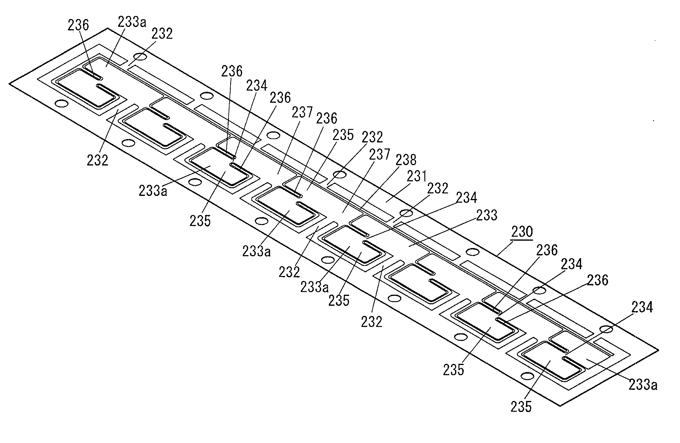
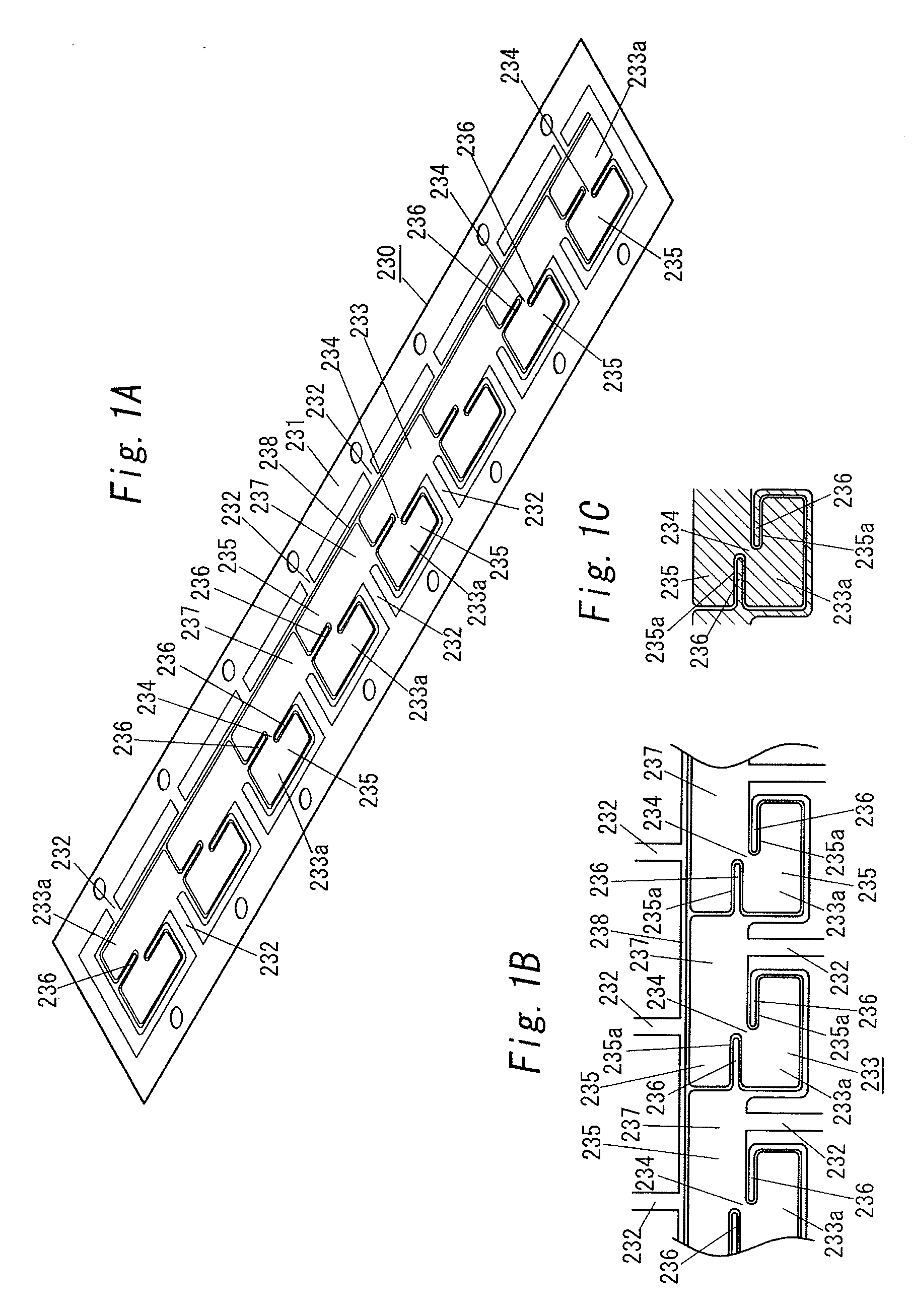
[0128]First, a lead frame is explained with reference to FIG. 1 to FIG. 3.

[0129]A lead frame 230 according to the present embodiment is the lead frame 230 in which a predetermined pattern 233 is supported inside of a one-pitch outer frame section 231 through support pieces 232. The lead frame 230 is formed using a band-shaped metal sheet 203 (see FIG. 4). The outer frame section 231 is formed in a rectangular frame shape, and the outer circumferential shape thereof is an elongated rectangle. In the band-shaped metal sheet 203 shown in FIG. 4, only a portion corresponding to one pitch of the lead frame 230 is shown, but this band-shaped metal sheet 203 may be configured of a portion of a metal hoop material. Further, in the present embodiment, the pattern 233 constitutes a wiring pattern.

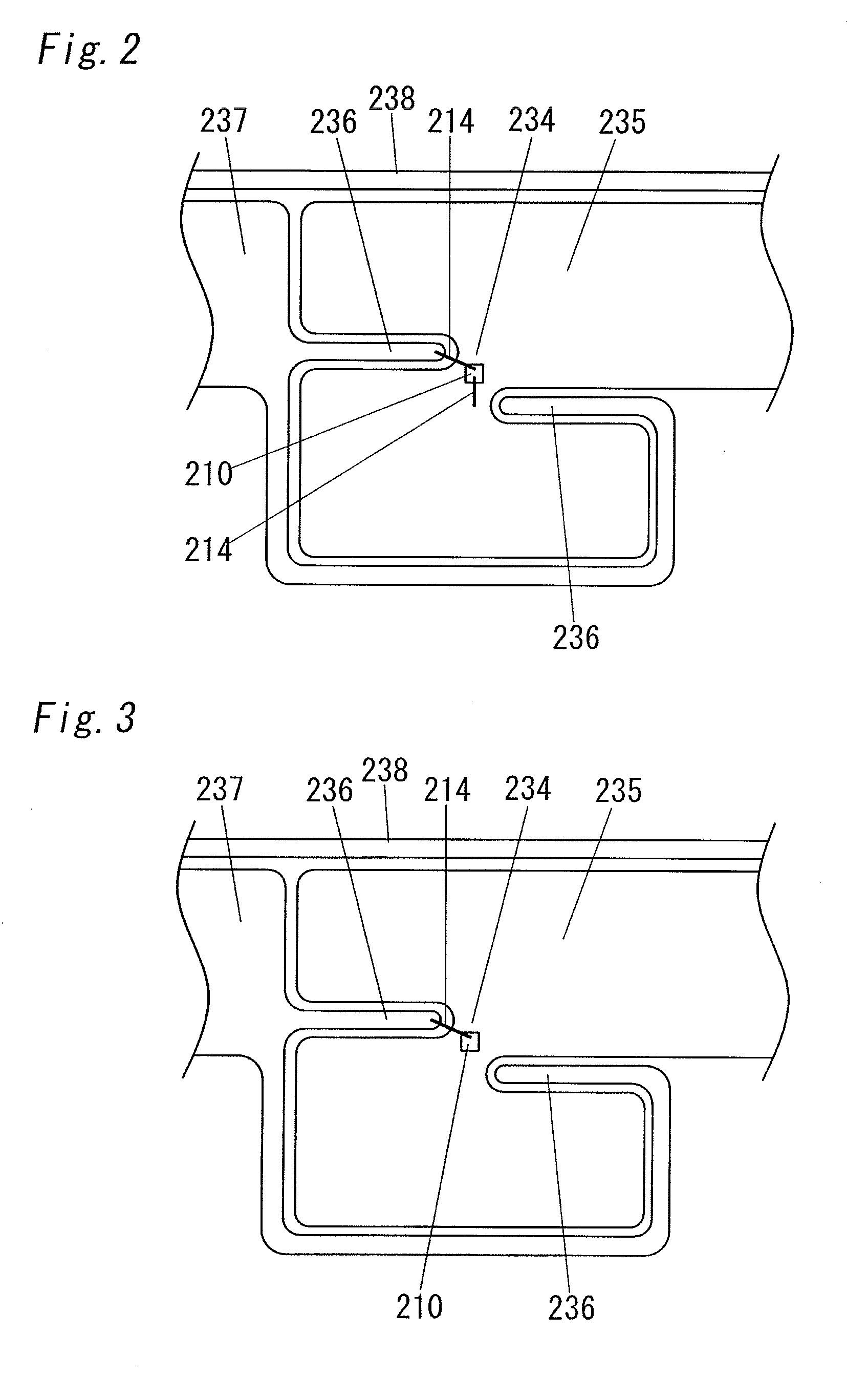
[0130]The pattern 233 of the lead frame 230 is provided with a plurality of base units 233a (in FIG. 1C, only one base unit 233a is shown by hatching), each of which includes a die pad 234 on which a...

embodiment 2

[0200]The basic configuration of the lead frame 230 of the present embodiment illustrated by FIG. 18A and FIG. 18B is substantially identical to that of Embodiment 1, the difference therebetween being that a plurality of basic units 233a are disposed so as to surround the center of the region surrounded by the outer frame section 231. The constituent elements same as those of Embodiment 1 are assigned with same reference numerals and the explanation thereof is herein omitted, as appropriate. FIG. 18A is a schematic perspective view of two-pitch sections of the lead frame 230.

[0201]In the lead frame 230 of the present embodiment, a plurality (ten in the example shown in the figure) of base units 233a is disposed separately on two concentric virtual circles, and the number of the die pads 234 on the virtual circle positioned relatively outside is larger than the number of the die pads 234 on the virtual circle positioned relatively inside. Therefore, in the wiring board 240 (see FIG. ...

embodiment 3

[0216]A light emitting unit 1 of the present embodiment is explained below with reference to FIG. 25 to FIG. 32.

[0217]The light emitting unit 1 comprises a mounting substrate 2 and a plurality of solid-state light emitting elements 3 disposed on one surface side of the mounting substrate 2.

[0218]The mounting substrate 2 comprises a heat transfer plate 21 having the solid-state light emitting elements 3 mounted on one surface side of the heat transfer plate 21, a wiring pattern 22 disposed on the other surface side of the heat transfer plate 21 and electrically connected to the solid-state light emitting elements 3, and an insulating layer 23 (first insulating layer 23) interposed between the heat transfer plate 21 and the wiring pattern 22. In this configuration, the heat transfer plate 21 is formed of the first metal plate, and the wiring pattern 22 is formed of a second metal plate with a linear expansion coefficient different from that of the first metal plate. The mounting subst...


PUM


Abstract

Provided is lead frame in which a wiring pattern supported by a support piece inside of a one-pitch outer frame section comprises a plurality of base units, each of which comprises a die pad on which a solid-state light emitting element is mounted, a heat sink extending from die pad so as to surround die pad electrically connected to one electrode of the element, and a lead electrically connected to the other electrode of the element. Lead of one base unit among adjacent base units and heat sink of the other base unit are coupled and electrically connected in series. Increase in temperature of the element is inhibited, light output is increased, and cost of a light emitting unit in which a plurality of solid-state light emitting elements connected in series are used is reduced. Also provided are wiring board, light emitting unit, and illuminating apparatus.

Description

TECHNICAL FIELD[0001]The present invention relates to a lead frame, a wiring board, a light emitting unit, and an illuminating apparatus.BACKGROUND ART[0002]A lead frame for use in the manufacture of a light-emitting device using an LED chip has been suggested (for example, Japanese Patent Application Publication No. 2006-93470; Patent Document 1).[0003]This Patent Document 1 describes, as shown in FIG. 60, a light emitting device 100 including a heat sink 160, an LED chip 161 mounted on the heat sink 160, a pair of lead sections 330 electrically connected by bonding wires 164a, 164b to the LED chip 161 and the heat sink 160, respectively, a resin package 400 that integrally supports the heat sink 100 and the lead sections 330 and allows the LED chip 161 to be exposed on the front surface side, and an attachment lens 560 that is mounted so as to cover the front surface side of the resin package 400 through a light-transmitting resin section 550.[0004]Further, Patent Document 1 also ...

Claims


Application Information

Patent Timeline
IPC IPC(8): F21V29/00F21V9/00
CPCH05K1/056F21V29/767H05K3/202F21Y2101/02F21Y2103/003F21Y2105/001H05K2201/10106F21K9/17F21K9/30F21K9/90F21V19/004H01L25/0753H01L33/486H01L33/62H05K1/0203H05K1/0271H01L2224/73265H05K1/181Y10S362/80F21V29/2256H01L2224/48227H01L2924/12041H01L24/45H01L2224/49113H01L2224/48228H01L2224/45124H01L2224/45144H01L2224/48091H01L2224/48137H01L2924/00014H01L2924/00H01L2924/12035H01L2924/12042H01L2924/181H01L24/97H01L2224/45139H01L2224/49171F21K9/20F21Y2105/10F21K9/27F21Y2103/10F21Y2115/10F21Y2107/90H01L2924/00011Y02P70/50H01L2924/00012H01L2924/01049H01L2224/45015H01L2924/207H01L33/64
Inventor URANO, YOJIYOKOTANI, RYOJIKUZUHARA, IKKOTANAKA, KENICHIRO
Owner PANASONIC INTELLECTUAL PROPERTY MANAGEMENT CO LTD
Why Eureka
Try Eureka