Lateral PNP Bipolar Transistor with Narrow Trench Emitter

a bipolar transistor and emitter technology, applied in the field of lateral bipolar transistors, can solve the problems of null the gain of the parasitic device, the performance of the existing lateral pnp bipolar transistor is typically limited,

Active Publication Date: 2013-03-28
ALPHA & OMEGA SEMICON INC
View PDF10 Cites 197 Cited by
  • Summary
  • Abstract
  • Description
  • Claims
  • Application Information

AI Technical Summary

Problems solved by technology

Lateral PNP bipolar transistors are known but existing lateral PNP bipolar transistors typically has limited performance.
Therefore, most existing lateral PNP transistor includes an N+ buried layer under the P-emitter where the high doping of the N+ buried layer effectively null the gain of the parasitic device.

Method used


Image

  • Lateral PNP Bipolar Transistor with Narrow Trench Emitter
  • Lateral PNP Bipolar Transistor with Narrow Trench Emitter
  • Lateral PNP Bipolar Transistor with Narrow Trench Emitter

Examples


first embodiment

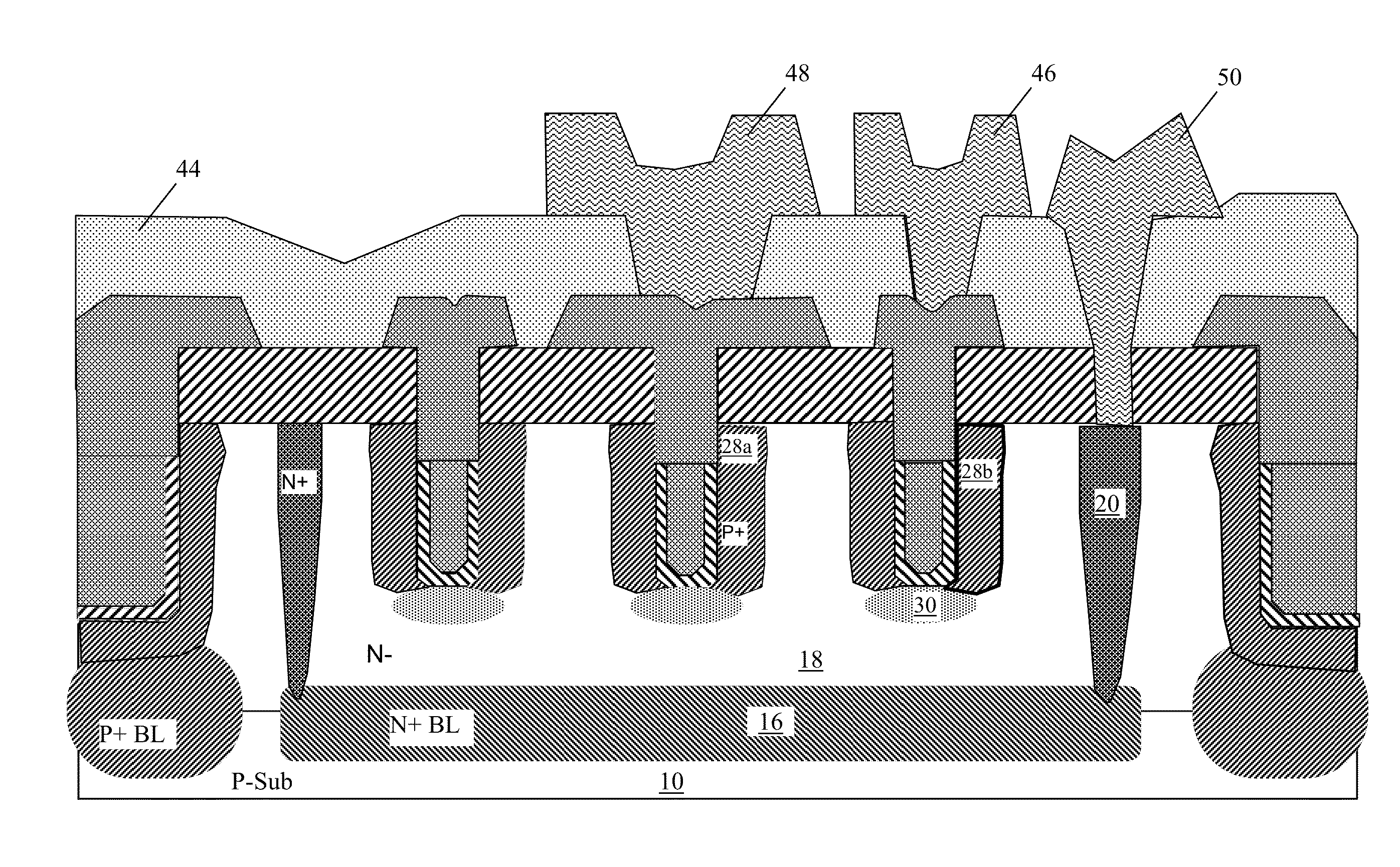
[0025]In the present invention, the trench emitter and trench collector are formed by ion implantation into the sidewall of trenches formed in a semiconductor layer. A bottom portion of the trench is lined with a thin sidewall oxide layer with the remaining portion filled with polysilicon. The thin sidewall oxide layer at the bottom portion of the trenches has the effect of preventing emitter-to-base breakdown at the bottom corners of the trenches.

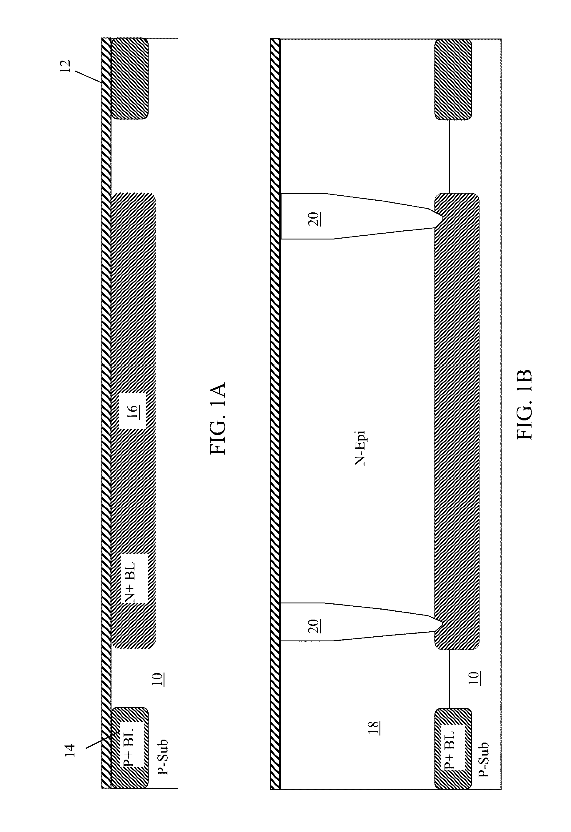
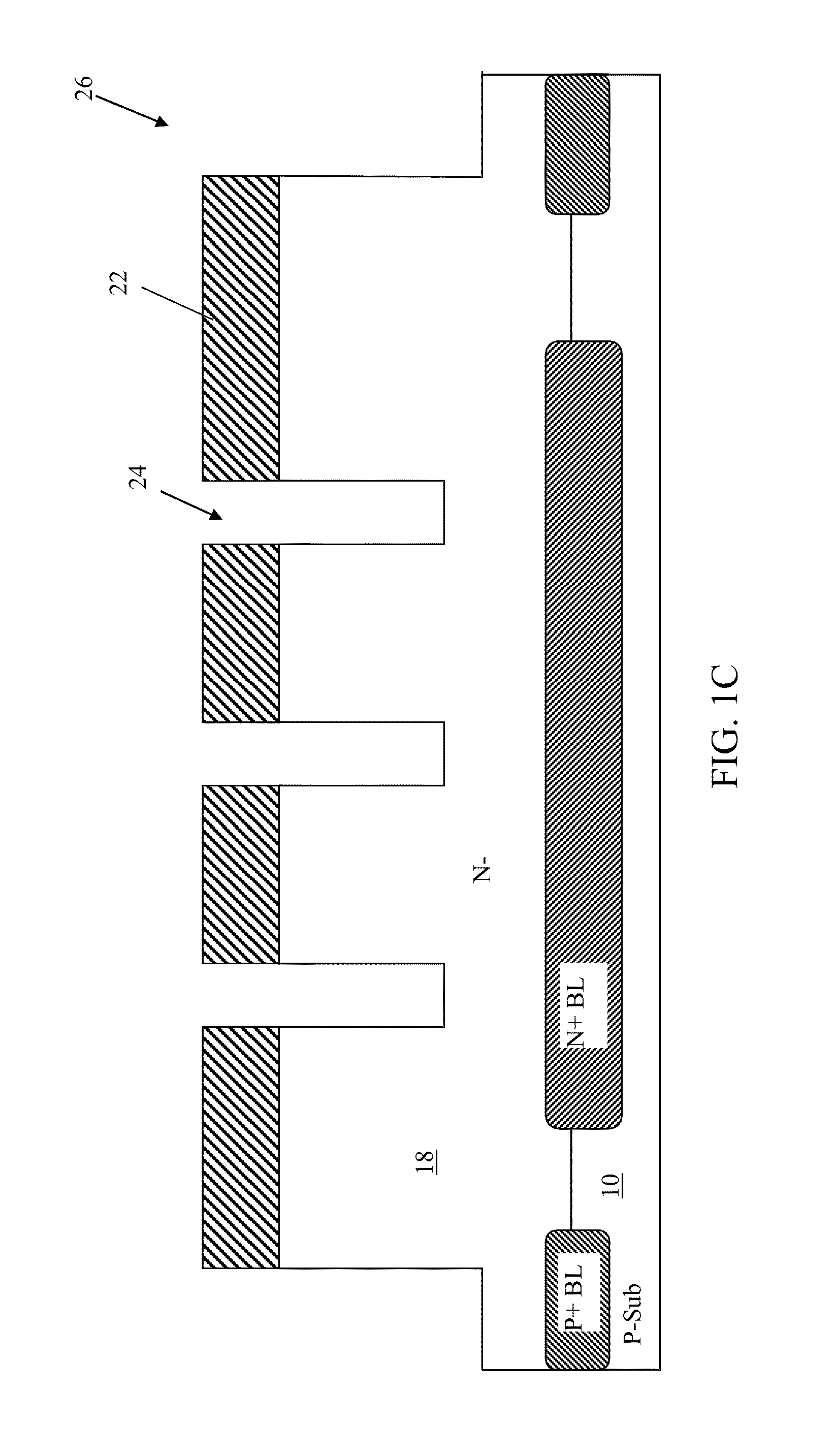
[0026]The fabrication process and the structure of the lateral PNP transistor of the present invention will now be described with reference to FIGS. 1A to 1K. Referring to FIGS. 1A to 1K, the lateral PNP transistor is formed on a P-type silicon substrate 10. A buffer oxide layer 12 may be formed on the top surface of the substrate 10 before the ion implantation steps that follow to form P+ buried layer 14 and N+ buried layer 16. The P+ buried layer 14 and the N+ buried layer 16 are formed using separate masking and ion implantation steps. ...

second embodiment

[0045]In the present invention, the trench emitter and trench collector are formed by filling trenches formed in a semiconductor layer with heavily doped polysilicon layer and auto-doping the trench sidewalls by out-diffusion of dopants from the doped polysilicon filler. An oxide layer is formed on the bottom portion of the trenches prior to polysilicon deposition. The oxide layer provides insulation and prevents emitter to base breakdown at the bottom corners of the trenches.

[0046]The fabrication process and the structure of the lateral PNP transistor of the present invention will now be described with reference to FIGS. 5A to 5J. Referring to FIGS. 5A to 5J, the lateral PNP transistor is formed on a P-type silicon substrate 10. A buffer oxide layer 12 may be formed on the top surface of the substrate 10 before the ion implantation steps that follow to form P+ buried layer 14 and N+ buried layer 16. The P+ buried layer 14 and the N+ buried layer 16 are formed using separate masking...


PUM


Abstract

A lateral bipolar transistor includes trench emitter and trench collector regions to form ultra-narrow emitter regions, thereby improving emitter efficiency. The same trench process is used to form the emitter/collector trenches as well as the trench isolation structures so that no additional processing steps are needed to form the trench emitter and collector. In embodiments of the present invention, the trench emitter and trench collector regions may be formed using ion implantation into trenches formed in a semiconductor layer. In other embodiments, the trench emitter and trench collector regions may be formed by out-diffusion of dopants from heavily doped polysilicon filled trenches.

Description

CROSS-REFERENCE TO RELATED APPLICATIONS[0001]The present application is related to concurrently filed and commonly assigned U.S. patent application entitled “Lateral PNP Bipolar Transistor Formed with Multiple Epitaxial Layers,” of the same inventors hereof, having patent application Ser. No. ______, which patent application is incorporated herein by reference in its entirety.FIELD OF THE INVENTION[0002]The invention relates to lateral bipolar transistors and, in particular, to lateral bipolar transistors with trench emitter and trench collector with narrow emitter regions to improve emitter efficiency.DESCRIPTION OF THE RELATED ART[0003]Lateral bipolar transistors include emitter and collector regions formed in a substrate functioning as the base of the transistor. The emitter and collector are formed such that lateral current flow in an area in the substrate relatively remote from the surface of the substrate. Lateral PNP bipolar transistors are known but existing lateral PNP bipo...

Claims


Application Information

Patent Timeline
Patent Type & Authority Applications(United States)
IPC IPC(8): H01L29/04H01L21/331
CPCH01L29/735H01L29/0808H01L29/6625H01L21/02532H01L21/02595H01L21/2254H01L21/31111H01L21/324H01L21/76224H01L29/0649
Inventor MALLIKARJUNASWAMY, SHEKARHEBERT, FRANCOIS
Owner ALPHA & OMEGA SEMICON INC
Why Eureka
Try Eureka