Heat treatment method for promoting crystallization of high dielectric constant film

Active Publication Date: 2013-03-28
DAINIPPON SCREEN MTG CO LTD
View PDF6 Cites 28 Cited by
  • Summary
  • Abstract
  • Description
  • Claims
  • Application Information

AI Technical Summary

Benefits of technology

[0012]The temperature of the front surface of the substrate is maintained near the target temperature with stability.
[0013]It is therefore an object of

Problems solved by technology

However, as gate insulator films are made thinner with the decreasing size of devices, the increase in leakage current has become a problem.
However, a problem to be described below arises during the heat treatment of a semiconductor wafer in which a high dielectric constant film is formed on a silicon-germa

Method used


Image

  • Heat treatment method for promoting crystallization of high dielectric constant film
  • Heat treatment method for promoting crystallization of high dielectric constant film
  • Heat treatment method for promoting crystallization of high dielectric constant film

Examples


Embodiment Construction

[0030]A preferred embodiment according to the present invention will now be described in detail with reference to the drawings.

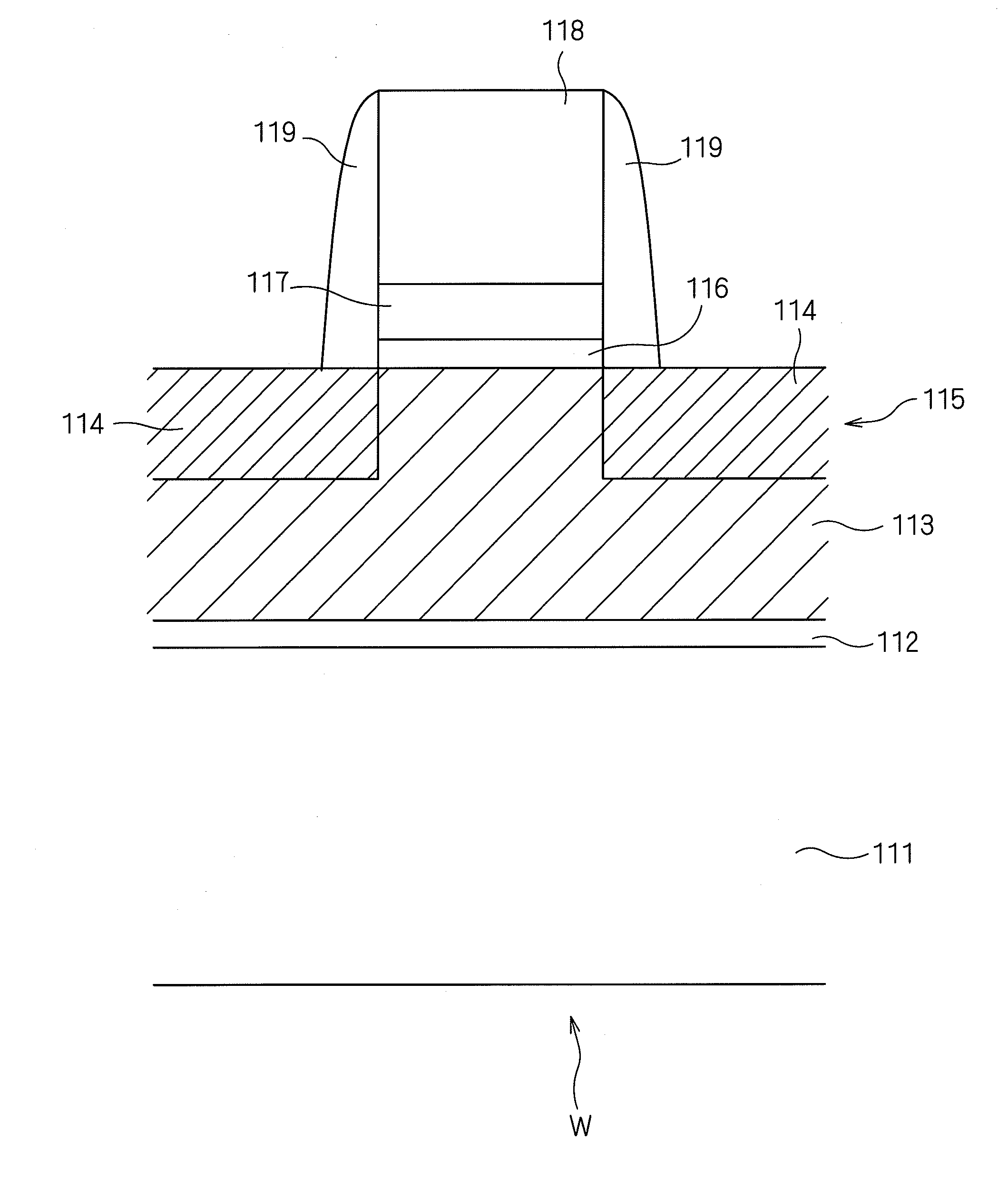
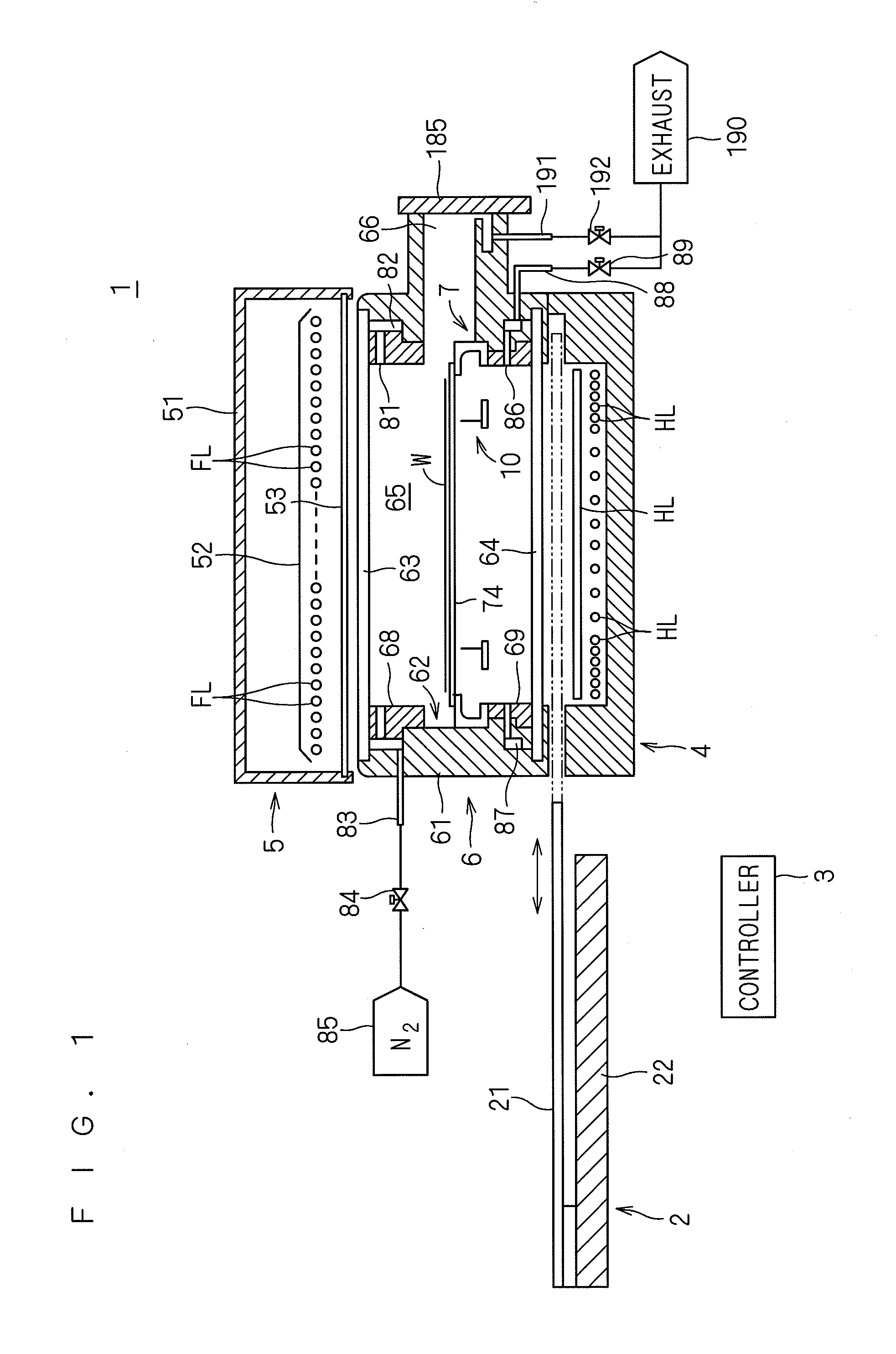
[0031]FIG. 1 is a longitudinal sectional view showing a configuration of a heat treatment apparatus 1 for carrying out a heat treatment method according to the present invention. The heat treatment apparatus 1 according to the present preferred embodiment is a flash lamp annealer for irradiating a disk-shaped semiconductor wafer W having a diameter of 300 mm and serving as a substrate with a flash of light to heat the semiconductor wafer W. A semiconductor wafer W prior to the transport into the heat treatment apparatus 1 includes a high dielectric constant film formed therein, and the heat treatment apparatus 1 performs a heating treatment on the semiconductor wafer W to thereby promote the crystallization of the high dielectric constant film, which will be described in detail later.

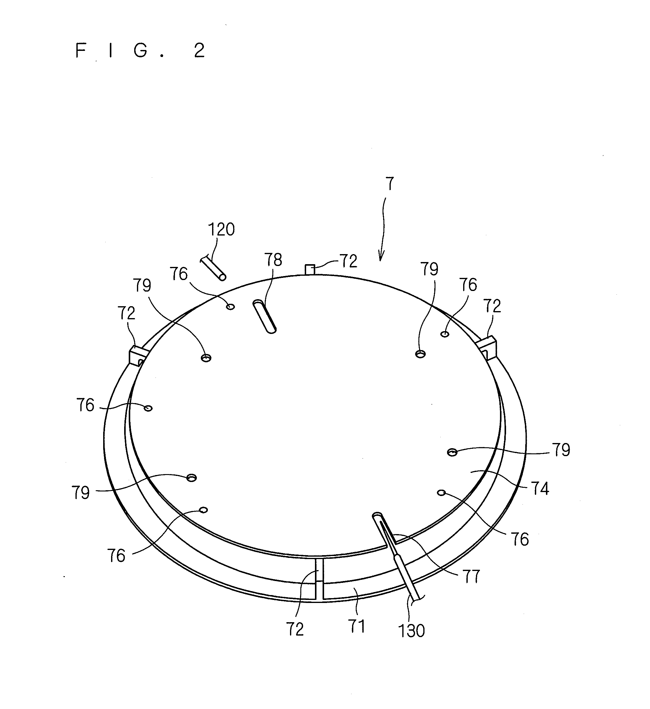
[0032]The heat treatment apparatus 1 includes a chamber 6 for receiving a s...


PUM


Abstract

A film of silicon dioxide is formed on the silicon-germanium layer, and a high dielectric constant film is further formed on the film of silicon dioxide. First irradiation from a flash lamp is performed on the semiconductor wafer to increase the temperature of a front surface of the semiconductor wafer from a preheating temperature to a target temperature for a time period in the range of 3 milliseconds to 1 second. Subsequently, second irradiation from the flash lamp is performed to maintain the temperature of the front surface of the semiconductor wafer within a ±25° C. range around the target temperature for a time period in the range of 3 milliseconds to 1 second. This promotes the crystallization of the high dielectric constant film while suppressing the alleviation of distortion in the silicon-germanium layer.

Description

BACKGROUND OF THE INVENTION[0001]1. Field of the Invention[0002]The present invention relates to a heat treatment method which heats a substrate such as a semiconductor wafer including a high dielectric constant film formed on a silicon-germanium layer to promote the crystallization of the high dielectric constant film.[0003]2. Description of the Background Art[0004]Hitherto, silicon dioxide (SiO2) has been typically used as the material of a gate insulator film for a field-effect transistor (FET). However, as gate insulator films are made thinner with the decreasing size of devices, the increase in leakage current has become a problem. To solve the problem, a metal gate electrode such that metal is used as the material of a gate electrode has been developed while a material (a high dielectric constant material) having a dielectric constant higher than that of silicon dioxide is used as the material of a gate insulator film, as disclosed in U.S. Patent Application Publication No. 20...

Claims


Application Information

Patent Timeline
IPC IPC(8): H01L21/3105H01L21/20
CPCH01L29/513H01L29/517H01L29/7848H01L21/2686H01L21/68735H01L21/02356H01L21/67115H01L21/68707H01L21/28176
Inventor FUSE, KAZUHIKOKATO, SHINICHI
Owner DAINIPPON SCREEN MTG CO LTD
Why Eureka
Try Eureka