Stack package

a technology of stacking and stacking components, applied in the field of stacking, can solve the problems of difficult to realize a capacitor having a large capacity, unreliable, and expensive methods of forming such capacitors, and achieve the effect of reducing power noise and cos

Inactive Publication Date: 2013-04-04
SK HYNIX INC
View PDF5 Cites 13 Cited by
  • Summary
  • Abstract
  • Description
  • Claims
  • Application Information

AI Technical Summary

Benefits of technology

[0011]Embodiments of the present invention include a stack package in which a capacitor for reducing power noise is reliably embedded at a reduced cost.
[0012]Also, embodiments of the present invention include a stack package which can realize a capacitor of a large capacity.
[0013]Further, embodiments of the present invention include a stack package which can prevent the volume of the package from increasing and accomplish the simplification of manufacturing processes.

Problems solved by technology

Known methods of forming such a capacitor are costly and are unreliable.
Further, according to the known methods, it is difficult to realize a capacitor having a large capacity, and therefore such capacitors have limitations in reducing power noise.
In addition, in the case of mounting the capacitor on the substrate, a problem is caused in that the volume of a package increases and a separate mounting process is needed.

Method used


Image

  • Stack package
  • Stack package
  • Stack package

Examples


Embodiment Construction

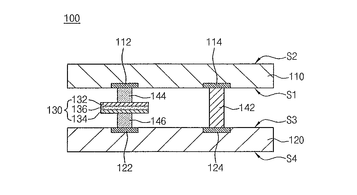
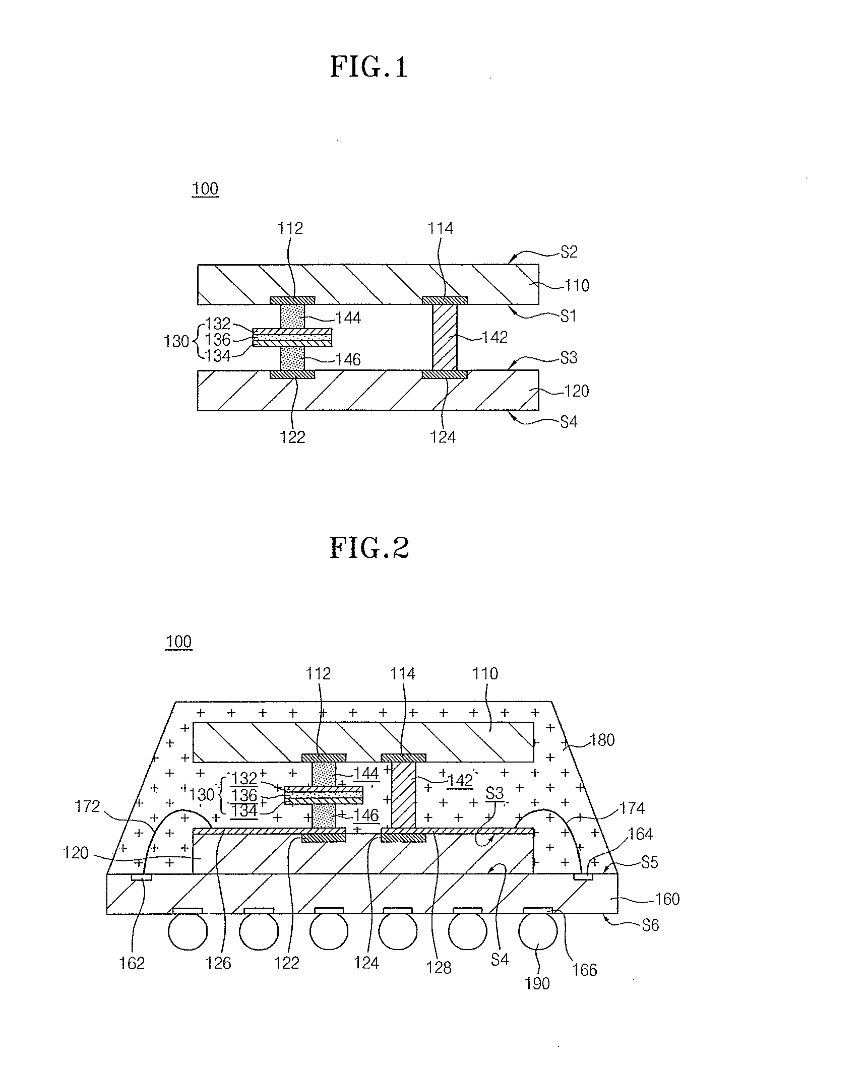
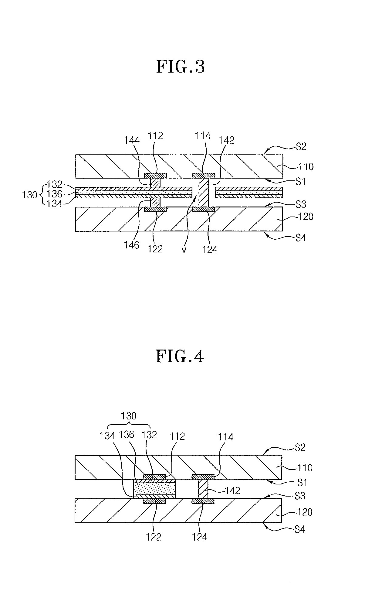
[0039]In the present invention, when realizing a stack package of a chip-on-chip structure, power pads and ground pads of an upper semiconductor chip and a lower semiconductor chip are connected by capacitors.

[0040]Therefore, according to embodiments of the present invention, even though the capacitors are embedded, the capacitors can be relatively simply formed, costs can be saved, and reliability can be secured.

[0041]Also, in the present invention, by freely adjusting the area of the electrodes of the capacitors, capacitors of a large capacity advantageous to the reduction of power noise can be easily realized.

[0042]Further, in the present invention, because the capacitors are disposed between the upper semiconductor chip and the lower semiconductor chip, the volume of the entire stack package is not unnecessarily increased.

[0043]Hereafter, specific embodiments of the present invention will be described in detail with reference to the accompanying drawings.

[0044]It is to be unders...


PUM


Abstract

A stack package includes a first semiconductor chip first pads and second pads disposed thereon and a second semiconductor chip having third pads and fourth pads electrically connected with the second pads disposed thereon. Capacitors are interposed between the first semiconductor chip and the second semiconductor chip, and include first electrodes electrically connected with the first pads of the first semiconductor chip, second electrodes electrically connected with the third pads of the second semiconductor chip, and dielectrics interposed between the first electrodes and the second electrodes.

Description

CROSS-REFERENCE TO RELATED APPLICATIONS[0001]The present application claims priority to Korean patent application number 10-2010-0010105 filed on Feb. 3, 2010, which is incorporated herein by reference in its entirety.BACKGROUND OF THE INVENTION[0002]The present invention relates generally to a stack package, and more particularly, to a stack package in which a capacitor is embedded to reduce power noise.[0003]A semiconductor package having a semiconductor chip capable of storing and / or processing a huge amount of data within a short period has been developed.[0004]It is known that stack a package, in which a plurality of semiconductor chips are stacked, increases data storage capacity. Further, a stack package is known, in which a memory semiconductor chip and a system semiconductor chip are stacked to increase a data storage capacity and also to improve a data processing speed.[0005]In order to maintain a data processing speed at a high level, it is necessary to minimize power noi...

Claims


Application Information

Patent Timeline
Patent Type & Authority Applications(United States)
IPC IPC(8): H01L27/08
CPCH01L27/0805H01L28/40H01L29/92H01L2224/16145H01L2224/48091H01L2924/00014H01L2224/16265H01L2224/0401H01L2224/04042H01L2224/1703H01L2224/48227H01L2224/73207H01L2924/15311H01L2924/19041H01L2924/19104H01L2224/06188H01L2224/02371H01L2224/32105H01L2224/171H01L24/05H01L24/06H01L24/08H01L24/13H01L24/16H01L24/17H01L24/48H01L24/73H01L2224/04026H01L2224/04073H01L2224/05548H01L2224/291H01L2224/32237H01L2224/73201H01L2224/73251H01L2224/08148H01L2224/08195H01L2224/08265H01L2224/16105H01L2924/181H01L24/29H01L24/32H01L2924/15312H01L2924/19103H01L2224/131H01L2224/08145H01L25/0657H01L2225/06513H01L2225/06565H01L2225/0651H01L2225/06527H01L23/642H01L2924/014H01L2224/10H01L2224/48H01L2224/08147
Inventor KIMPARK, MYUNG GEUN
Owner SK HYNIX INC
Why Eureka
Try Eureka