
Passive Probing of Various Locations in a Wireless Enabled Integrated Circuit (IC)

a wireless enabled integrated circuit and functional module technology, applied in the field of wireless communication among functional modules of integrated circuits, can solve problems such as the problem of affecting the communication between integrated circuits at these increased data rates, frequencies and/or distances, and the use of conductive wires and/or traces for communication

Inactive Publication Date: 2013-04-04
AVAGO TECH INT SALES PTE LTD
View PDF17 Cites 5 Cited by
  • Summary
  • Abstract
  • Description
  • Claims
  • Application Information

AI Technical Summary

Benefits of technology

The present invention relates to integrating multiple functional modules in an integrated circuit using a waveguide to wirelessly communicate among them. The invention addresses the problem of degraded communication among the integrated circuits at increased data rates and frequencies due to the shortcomings of conductive wires and traces. The invention provides a solution for interconnecting integrated circuits over longer distances at increased data rates and frequencies. The technical effects of the invention include improved wireless communication among the integrated circuits, reduced parasitic capacitance and inductance, and improved performance and reliability of the integrated circuit.

Problems solved by technology

However, as the data rates, the frequencies, and / or the distances increase, physical properties of the conductive wires and / or traces may degrade communication among the integrated circuits.
For example, an undesirable or a parasitic capacitance and / or inductance of the conductive wires and / or traces may degrade communication among the integrated circuits at these increased data rates, frequencies, and / or distances.
Electronic designers are creating new electronic devices that include more integrated circuits that communicate at increased data rates and / or frequencies and over longer distances thereby making the use of conductive wires and / or traces for communication problematic.

Method used


Image

  • Passive Probing of Various Locations in a Wireless Enabled Integrated Circuit (IC)
  • Passive Probing of Various Locations in a Wireless Enabled Integrated Circuit (IC)
  • Passive Probing of Various Locations in a Wireless Enabled Integrated Circuit (IC)

Examples


Embodiment Construction

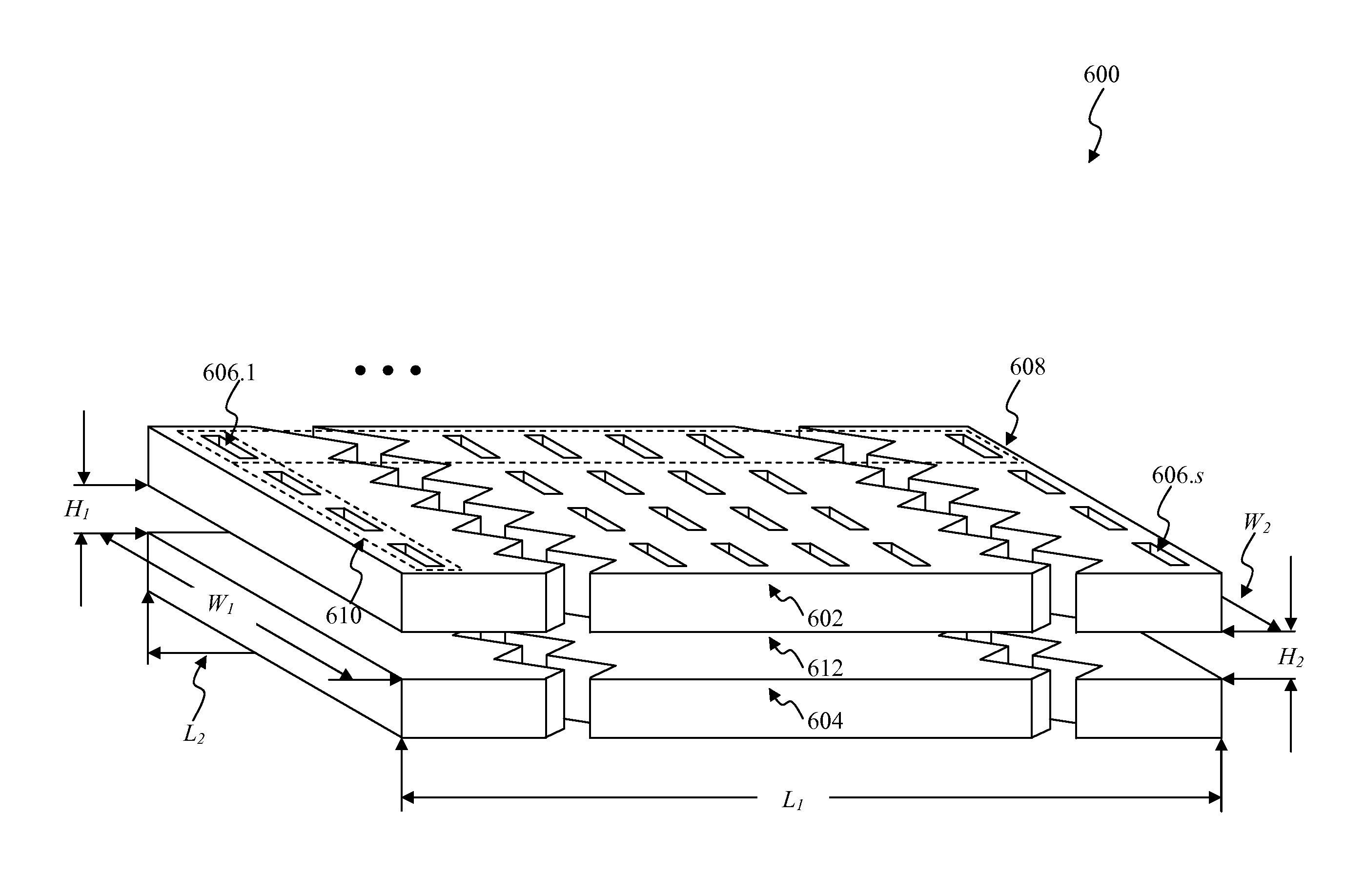
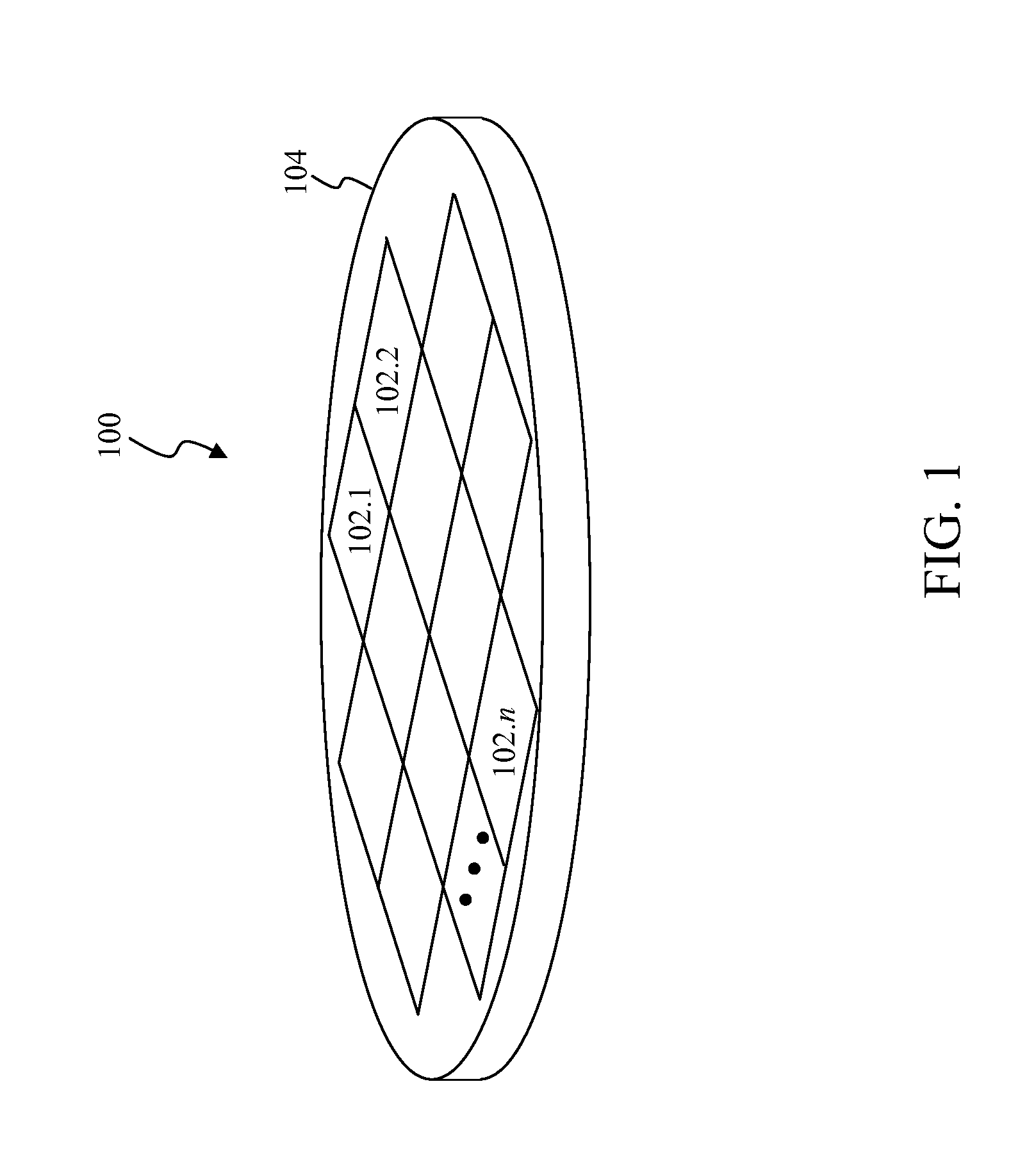
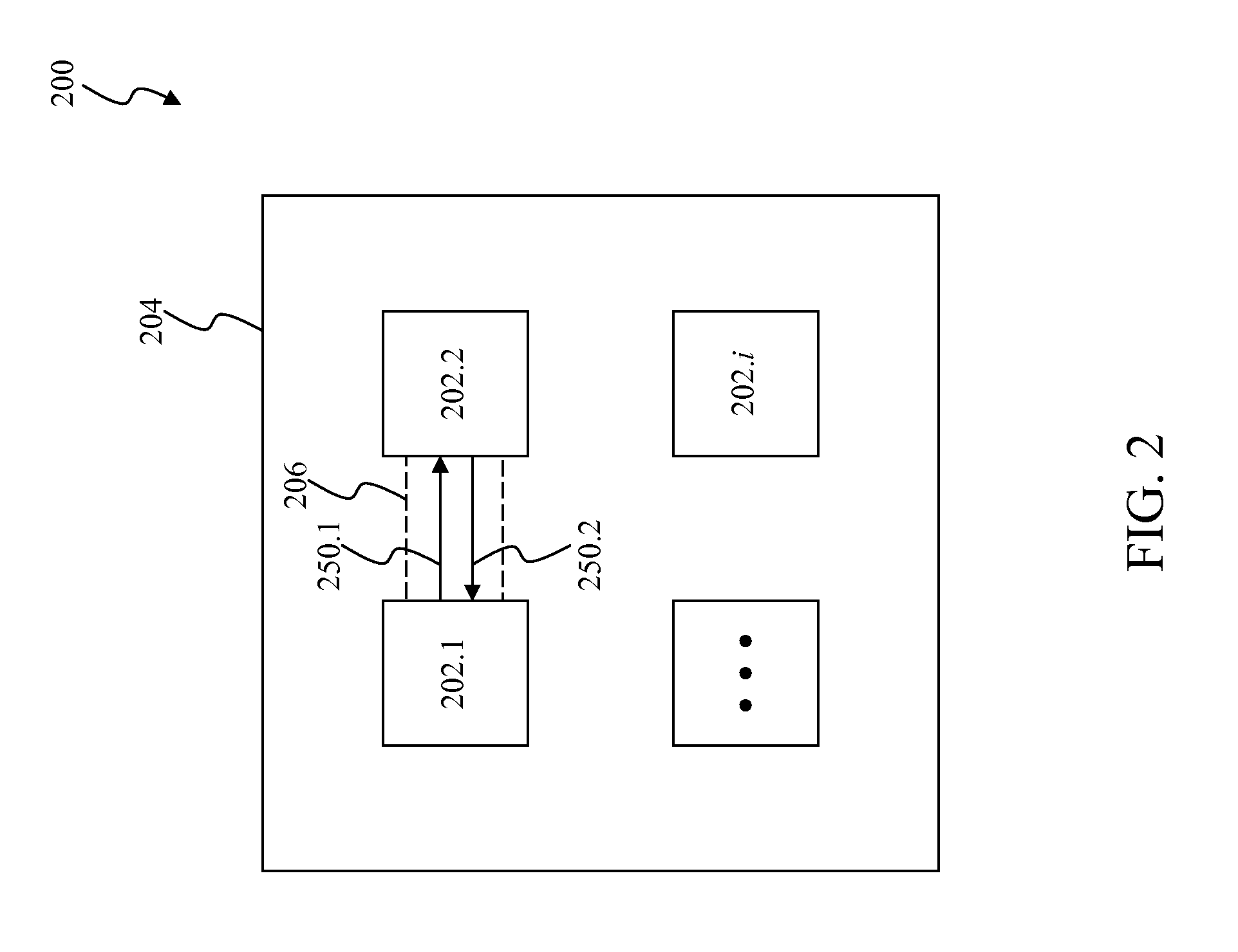
[0038]The following Detailed Description refers to accompanying drawings to illustrate exemplary embodiments consistent with the invention. References in the Detailed Description to “one exemplary embodiment,”“an exemplary embodiment,”“an example exemplary embodiment,” etc., indicate that the exemplary embodiment described may include a particular feature, structure, or characteristic, but every exemplary embodiment may not necessarily include the particular feature, structure, or characteristic. Moreover, such phrases are not necessarily referring to the same exemplary embodiment. Further, when a particular feature, structure, or characteristic is described in connection with an exemplary embodiment, it is within the knowledge of those skilled in the relevant art(s) to affect such feature, structure, or characteristic in connection with other exemplary embodiments whether or not explicitly described.

[0039]The exemplary embodiments described herein are provided for illustrative purp...


PUM


Abstract

Methods and apparatus are disclosed for wirelessly communicating among integrated circuits and / or functional modules within the integrated circuits. A semiconductor device fabrication operation uses a predetermined sequence of photographic and / or chemical processing steps to form one or more functional modules onto a semiconductor substrate. The functional modules are coupled to an integrated waveguide that is formed onto the semiconductor substrate and / or attached thereto to form an integrated circuit. The functional modules communicate with each other as well as to other integrated circuits using a multiple access transmission scheme via the integrated waveguide. One or more integrated circuits may be coupled to an integrated circuit carrier to form Multichip Module. The Multichip Module may be coupled to a semiconductor package to form a packaged integrated circuit.

Description

BACKGROUND[0001]1. Field of Invention[0002]Generally, the present invention relates to wireless communication among functional modules of an integrated circuit, and specifically, to integrating a waveguide with the functional modules to wirelessly communicate using a multiple access transmission scheme.[0003]2. Related Art[0004]A semiconductor device fabrication operation is commonly used to manufacture integrated circuits onto a semiconductor substrate to form a semiconductor wafer. Integrated circuits from among various semiconductor wafers are often packaged together to form an electronic device, such as a mobile device or a personal computing device to provide some examples. These integrated circuits are often interconnected to each other using conductive wires and / or traces and communicate among themselves using these conductive wires and / or traces.[0005]Typically, the conductive wires and / or traces are suitable for communication among the integrated circuits when low data rate...

Claims


Application Information

Patent Timeline
Patent Type & Authority Applications(United States)
IPC IPC(8): G01R31/26
CPCG01R31/3025G01R31/303G01R31/2831G01R31/2822H01L2224/16225H01L2924/15311G01R31/2834
Inventor CASTANEDA, JESUS ALFONSOBEHZAD, ARYA REZAROFOUGARAN, AHMADREZAZHAO, SAM ZIQUNBOERS, MICHAEL
Owner AVAGO TECH INT SALES PTE LTD
Learn More