Graphene and Nanotube/Nanowire Transistor with a Self-Aligned Gate Structure on Transparent Substrates and Method of Making Same

Active Publication Date: 2013-05-02
GLOBALFOUNDRIES US INC
View PDF9 Cites 41 Cited by
  • Summary
  • Abstract
  • Description
  • Claims
  • Application Information

AI Technical Summary

Problems solved by technology

One challenge for implementation of such carbon-based devices, however, is that there currently exists no practical method to fabricate a self-align

Method used


Image

  • Graphene and Nanotube/Nanowire Transistor with a Self-Aligned Gate Structure on Transparent Substrates and Method of Making Same
  • Graphene and Nanotube/Nanowire Transistor with a Self-Aligned Gate Structure on Transparent Substrates and Method of Making Same
  • Graphene and Nanotube/Nanowire Transistor with a Self-Aligned Gate Structure on Transparent Substrates and Method of Making Same

Examples


Embodiment Construction

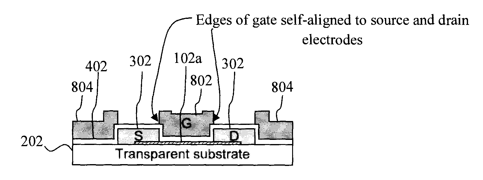
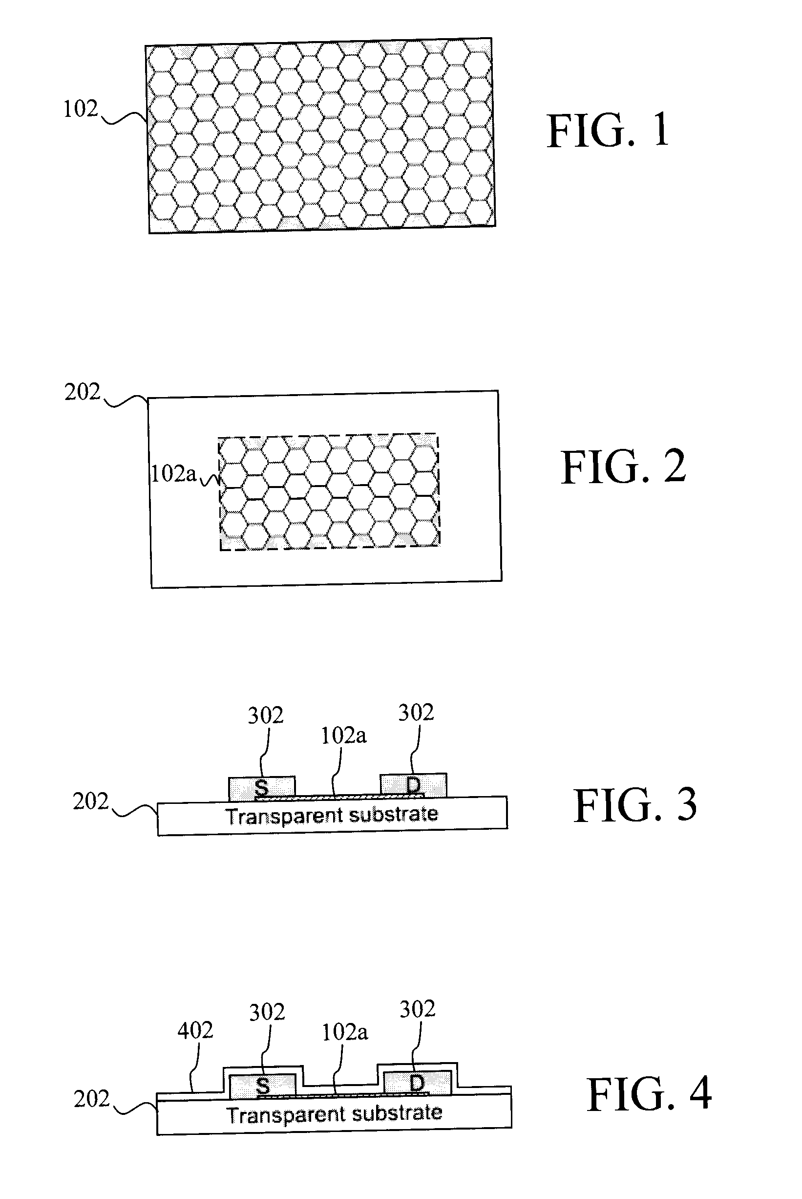
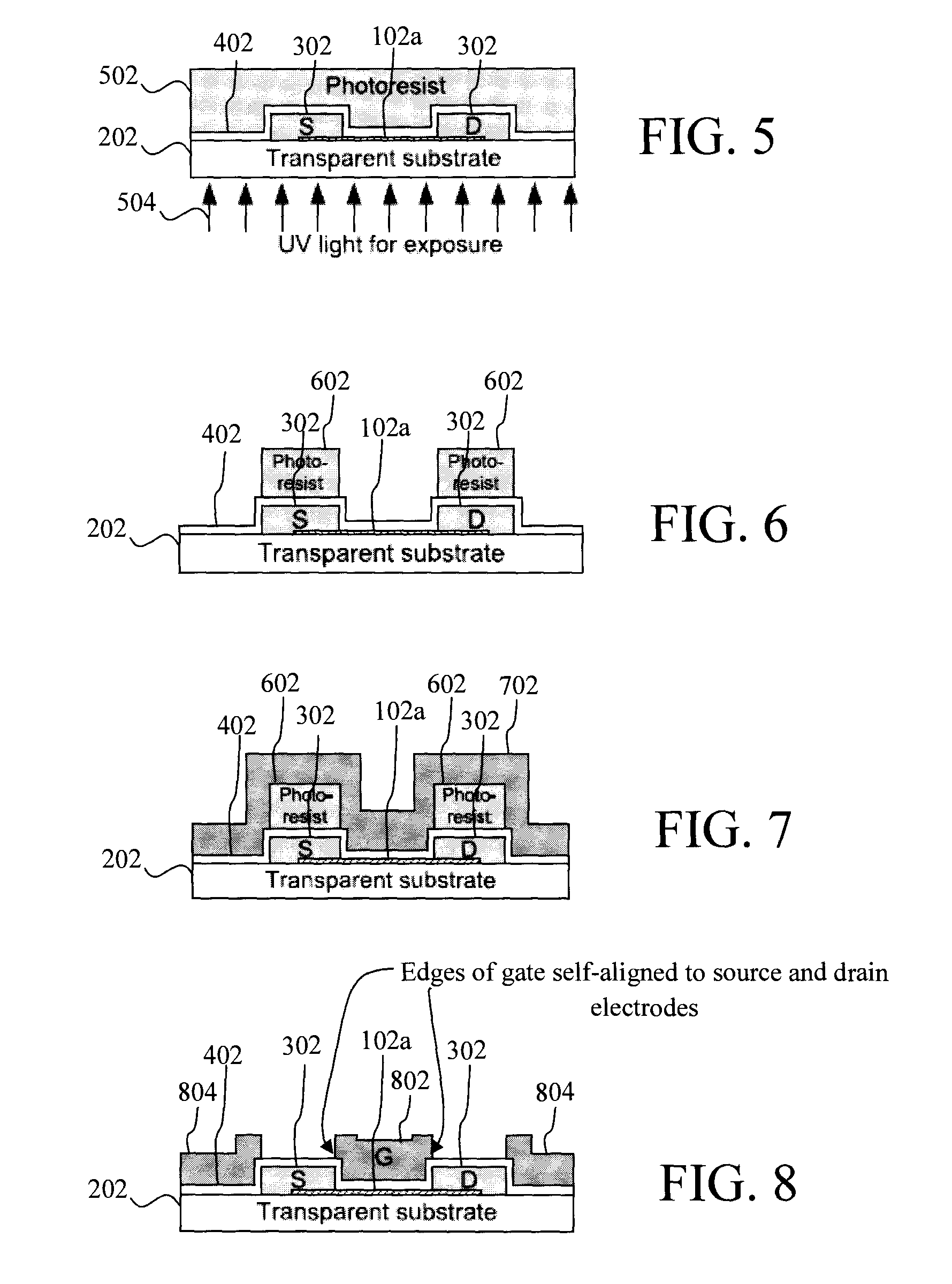
[0025]Provided herein are transistor devices with a self-aligned gate structure fabricated on transparent substrates. FIGS. 1-9 illustrate an exemplary methodology for fabricating such devices.

[0026]FIG. 1 is a top-down diagram illustrating a channel material 102 having been formed on a transparent substrate. In the depiction of FIG. 1, the transparent substrate is obscured by the channel material and thus is not visible. However, the transparent substrate is shown in illustrated in subsequent figures.

[0027]According to an exemplary embodiment, the channel material is made up of one of a carbon-based material, such as graphene or carbon nanotubes. Graphene is a one atom thick sheet of carbon atoms that are arranged in a honeycomb crystal lattice structure. See, for example, FIGS. 1 and 2. While FIGS. 1 and 2 illustrate graphene as the channel material, as highlighted above, graphene is only one of a number of different exemplary channel materials that may be used in accordance with ...


PUM


Abstract

Transistor devices having a self-aligned gate structure on transparent substrates and techniques for fabrication thereof are provided. In one aspect, a method of fabricating a transistor device includes the following steps. A channel material is formed on a transparent substrate. Source and drain electrodes are formed in contact with the channel material. A dielectric layer is deposited on the channel material. A photoresist is deposited on the dielectric layer and developed using UV light exposure through the transparent substrate. A gate metal(s) is deposited on the exposed portions of the dielectric layer and the undeveloped portions of the photoresist. The undeveloped portions of the photoresist are removed along with portions of the gate metal over the source and drain regions to form a gate of the device on the dielectric layer over the channel material which is self-aligned to the source and drain electrodes.

Description

STATEMENT OF GOVERNMENT RIGHTS[0001]This invention was made with Government support under Contract number FA8650-08-C-7838 awarded by (DARPA) Defense Advanced Research Projects Agency. The Government has certain rights in this invention.FIELD OF THE INVENTION[0002]The present invention relates to transistor devices and more particularly, to transistor devices having a self-aligned gate structure on transparent substrates and techniques for fabrication thereof.BACKGROUND OF THE INVENTION[0003]Transistors used for integrated circuits require minimal parasitic capacitance to maximize the circuit speed and frequency. Each transistor typically includes a source region and a drain region interconnected by a channel and a gate that regulates electron flow through the channel. To minimize parasitic capacitance, traditional silicon metal-oxide semiconductor field effect transistors (MOSFETs) can employ self-aligned gate structures. Specifically, with these structures, the gate is self aligne...

Claims


Application Information

Patent Timeline
IPC IPC(8): H01L29/772H01L21/336H01L29/775B82Y40/00B82Y99/00
CPCH01L29/42364H01L29/43H01L29/66431H01L29/7781H01L29/1606H01L21/2686H01L21/283H01L21/308H01L29/1608H01L29/66068H01L29/66515H01L29/66742H01L29/78684H01L29/0669H01L29/122H01L29/42376H01L29/42312H01L29/66568
Inventor HAENSCH, WILFRIED ERNST-AUGUSTLIU, ZIHONG
Owner GLOBALFOUNDRIES US INC
Why Eureka
Try Eureka