Solid-state imaging device

Active Publication Date: 2013-05-02
HAMAMATSU PHOTONICS KK
View PDF11 Cites 4 Cited by
  • Summary
  • Abstract
  • Description
  • Claims
  • Application Information

AI Technical Summary

Benefits of technology

[0026]Moreover, in the solid-state imaging device, the heat transfer member may form a part of a vacuum vessel, the solid-state imaging element and the first semiconductor element may be arranged in the vacuum vessel, and the cooling structure may be arranged out of the vacuum vessel. By such a configuration, detection objects including electron beams and X-rays that are generated in the vacuum v

Problems solved by technology

Moreover, if the imaging plane has a wider width in the horizontal direction, the distance between a pixel farthest from an amplifier circuit and the amplifier circuit becomes longer, which causes an increase in noise to be contained in an output signal.
In the case of, for example, an inspection of a semiconductor element structure built on a semiconductor wafer, imaging of a minute area (for

Method used


Image

  • Solid-state imaging device
  • Solid-state imaging device
  • Solid-state imaging device

Examples


Embodiment Construction

[0036]Hereinafter, embodiments of a solid-state imaging device according to the present invention will be described in detail with reference to the accompanying drawings. Also, the same components will be denoted with the same reference numerals in the description of the drawings, and overlapping description will be omitted.

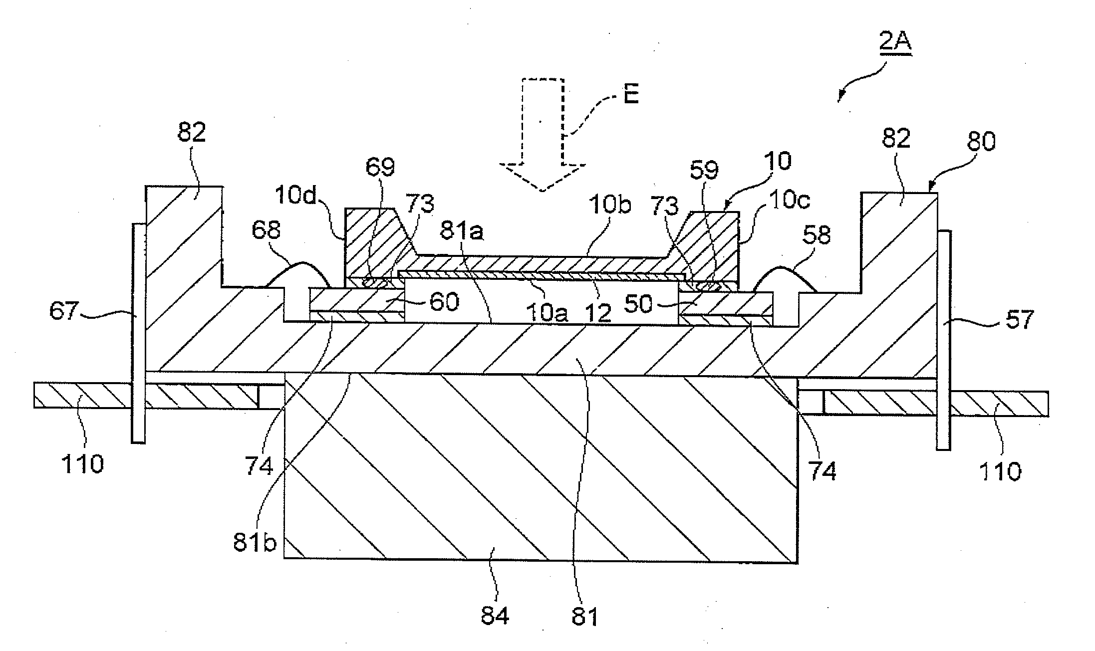
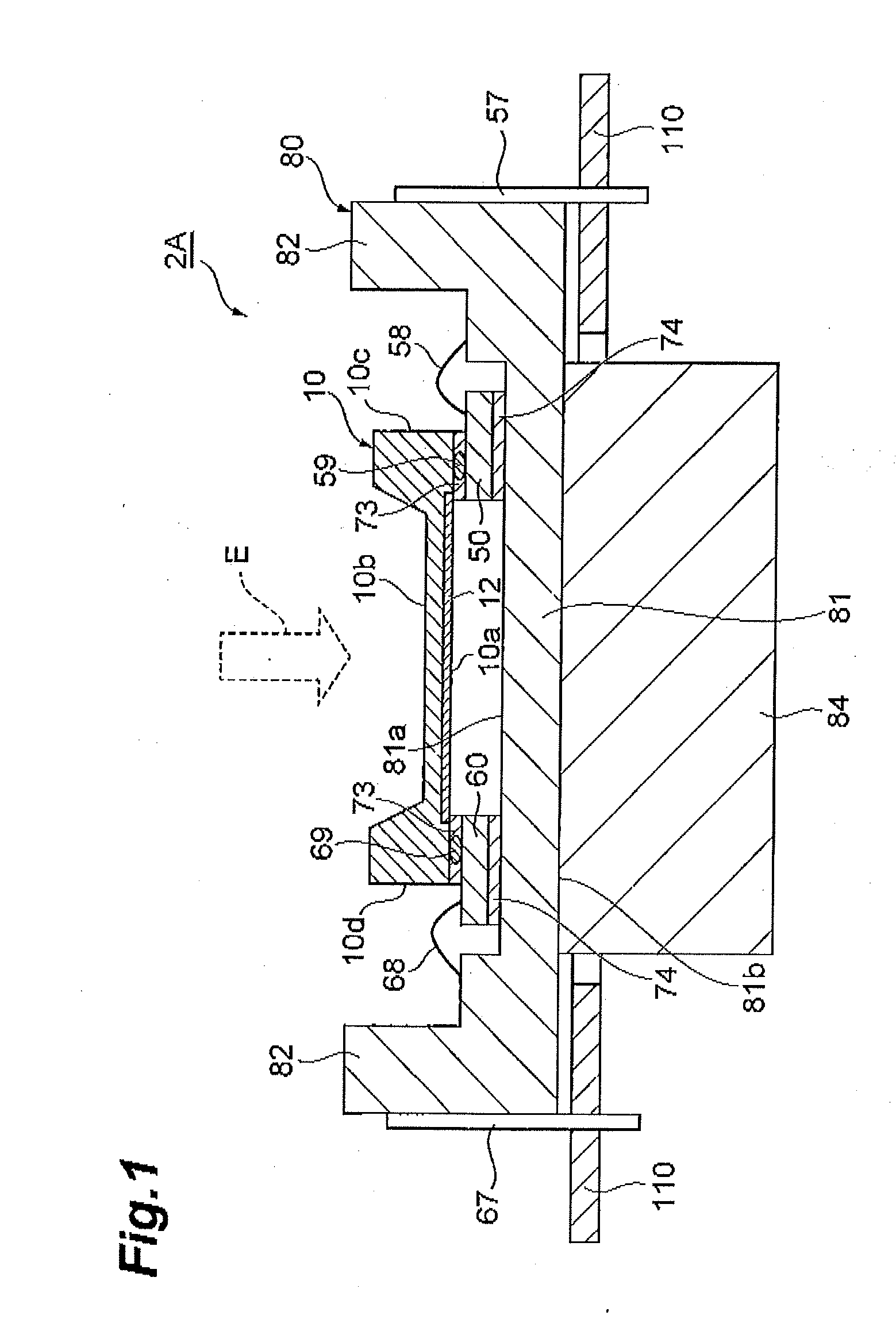
[0037]FIG. 1 is a side sectional view showing a configuration of a solid-state imaging device 2A according to an embodiment of the present invention. As shown in FIG. 1, the solid-state imaging device 2A includes a solid-state imaging element 10, two semiconductor elements 50 and 60, a heat transfer member 80, a cooling block 84, and a circuit board 110.

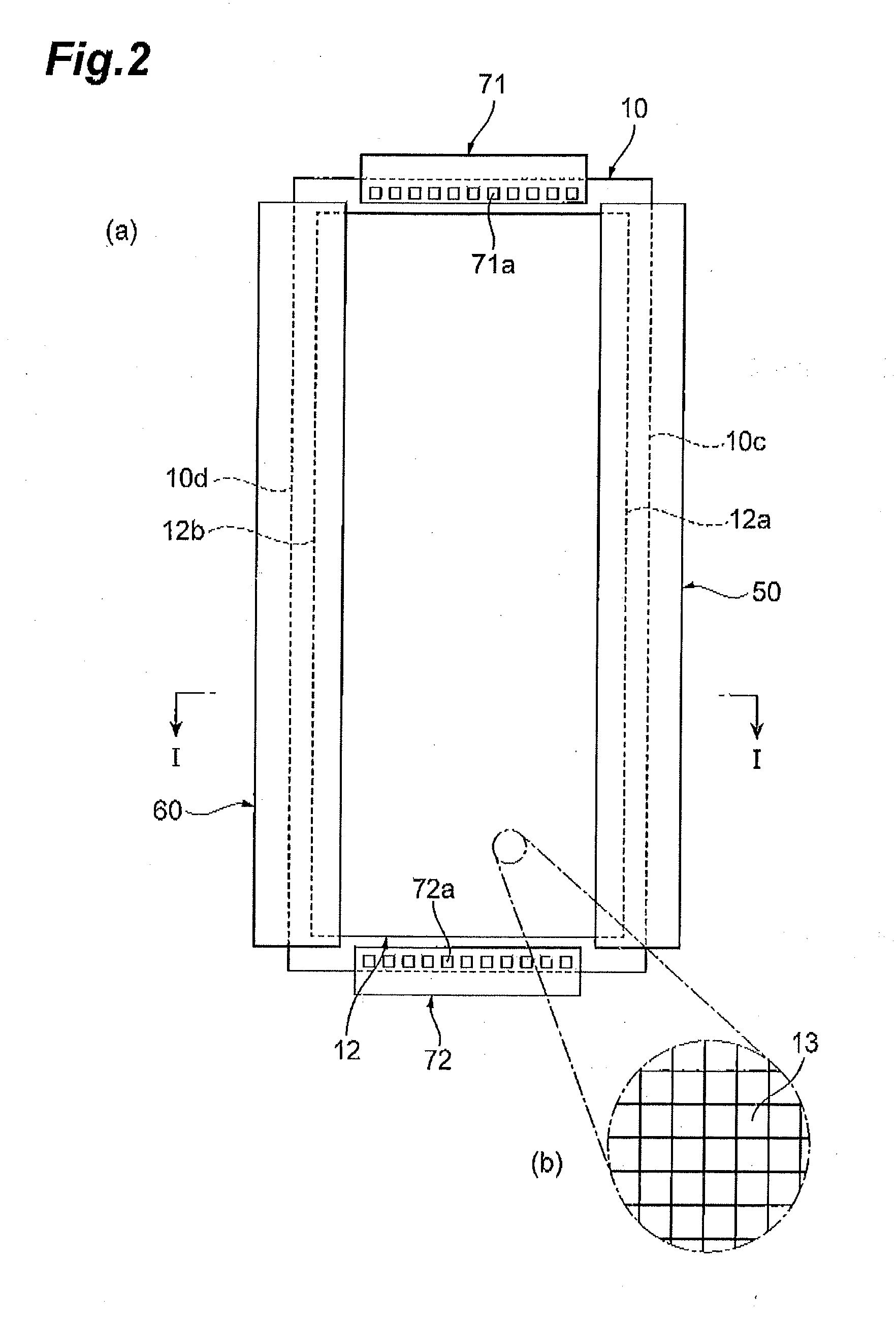
[0038]FIG. 2(a) is a plan view showing a configuration of the solid-state imaging element 10 and the two semiconductor elements 50 and 60. FIG. 2(b) is a partially enlarged view of FIG. 2(a). Also, FIG. 1 shows a section taken along a line I-I of the solid-state imaging device 2A shown in FIG. 2.

[0039]The solid-st...


PUM


Abstract

A solid-state imaging device 2A includes a CCD-type solid-state imaging element 10 having an imaging plane 12 formed of M×N pixels that are two-dimensionally arrayed in M rows and N columns and N signal readout circuits 20 arranged on one end side in the column direction for each of the columns with respect to the plane 12 and for outputting electrical signals according to the magnitudes of charges taken out of the respective columns, respectively, a C-MOS-type semiconductor element 50 for digital-converting and sequentially outputting as serial signals electrical signals output from the circuits 20 for each of the columns, a heat transfer member 80 having a main surface 81a and a back surface 81b, and a cooling block 84 provided on the surface 81b, and the semiconductor element 50 and the surface 81a of the heat transfer member 80 are bonded to each other.

Description

BACKGROUND OF THE INVENTION[0001]1. Field of the Invention[0002]The present invention relates to a solid-state imaging device.[0003]2. Related Background Art[0004]Japanese Patent Application Laid-Open No. 2002-135656 discloses a solid-state imaging device including an interline CCD architecture section. This solid-state imaging device includes a plurality of charge detection circuits each for converting a charge output from a charge transfer CCD to a voltage signal and a horizontal scanning circuit for sequentially reading out voltage signals output from these charge detection circuits. The horizontal scanning circuit is formed by a CMOS circuit to perform a high-speed readout operation.[0005]Japanese Patent Application Laid-Open No. 2007-19664 discloses a solid-state imaging device including an interline CCD architecture section. This solid-state imaging device includes a pixel array region for which a plurality of photoelectric conversion units are arrayed into rows and columns, v...

Claims


Application Information

Patent Timeline
IPC IPC(8): H04N5/335
CPCH01L27/14618H04N5/2253H01L2224/16H01L2224/48091H04N23/54H01L2924/00014
Inventor SUYAMA, MOTOHIROUJIMA, AKIOMIMAETA, KENTAROSUZUKI, HISANORIMURAMATSU, MASAHARUIWASE, FUMIO
Owner HAMAMATSU PHOTONICS KK
Why Eureka
Try Eureka