Imaging device

Active Publication Date: 2013-05-02
PANASONIC INTELLECTUAL PROPERTY MANAGEMENT CO LTD
View PDF1 Cites 13 Cited by
  • Summary
  • Abstract
  • Description
  • Claims
  • Application Information

AI Technical Summary

Benefits of technology

[0016]As described above, in the imaging device of the present disclosure, since a potential in the second ground conductor of the imaging sensor cable becomes stable, also when the imaging device is used in an intense electric field environment, image interference cause

Problems solved by technology

In a case where the imaging device is used in such an environment, the imaging device is likely to be subjected to an electromagnetic interference.
If an imaging device such as a digital still camera is used in the intense electric field environment, an image taken by the imaging device may contain a stripe pattern noise (beat noise), and image interference may be caused.
The higher a performance of an imaging sensor

Method used


Image

  • Imaging device
  • Imaging device
  • Imaging device

Examples


Example

First Embodiment

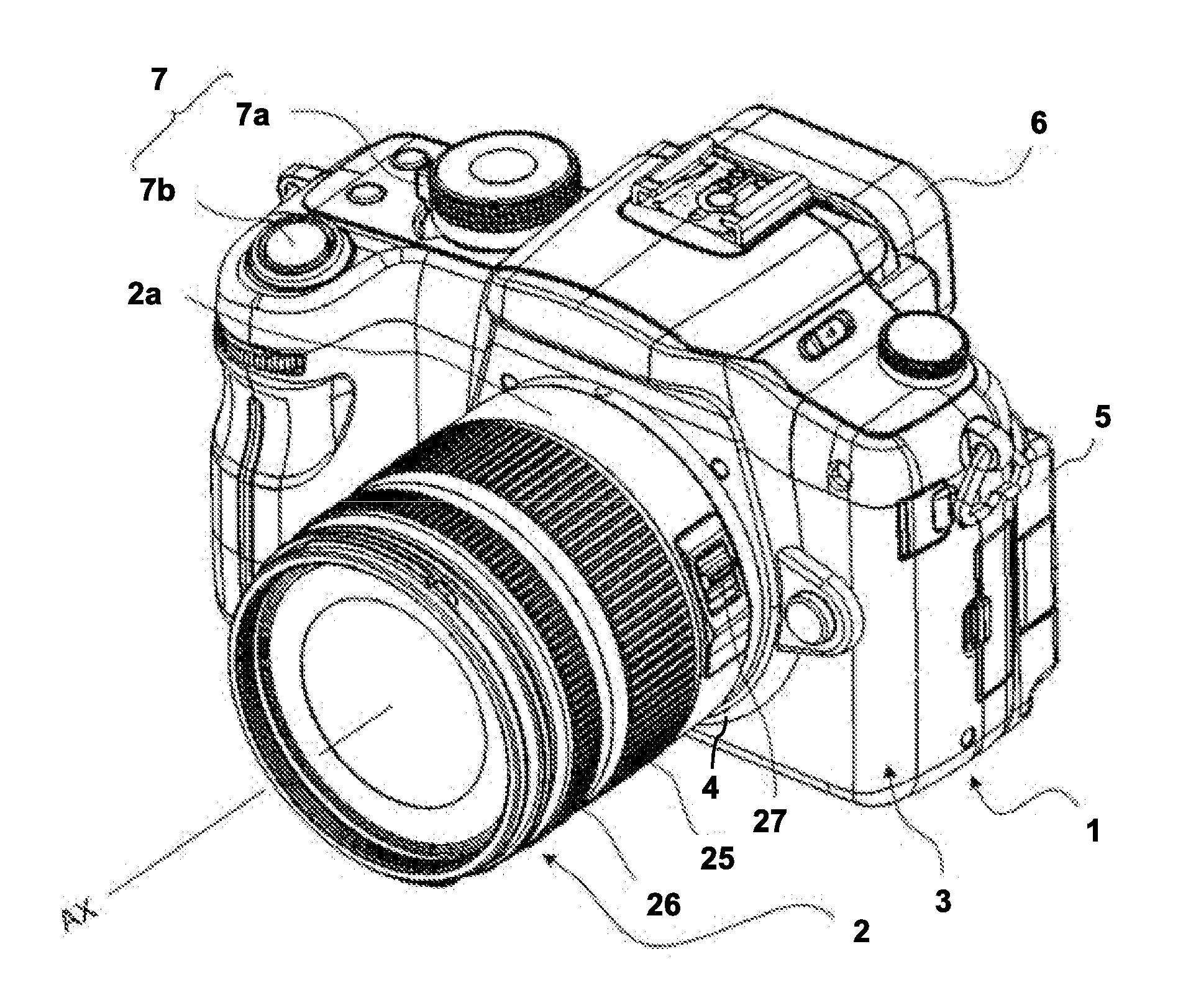
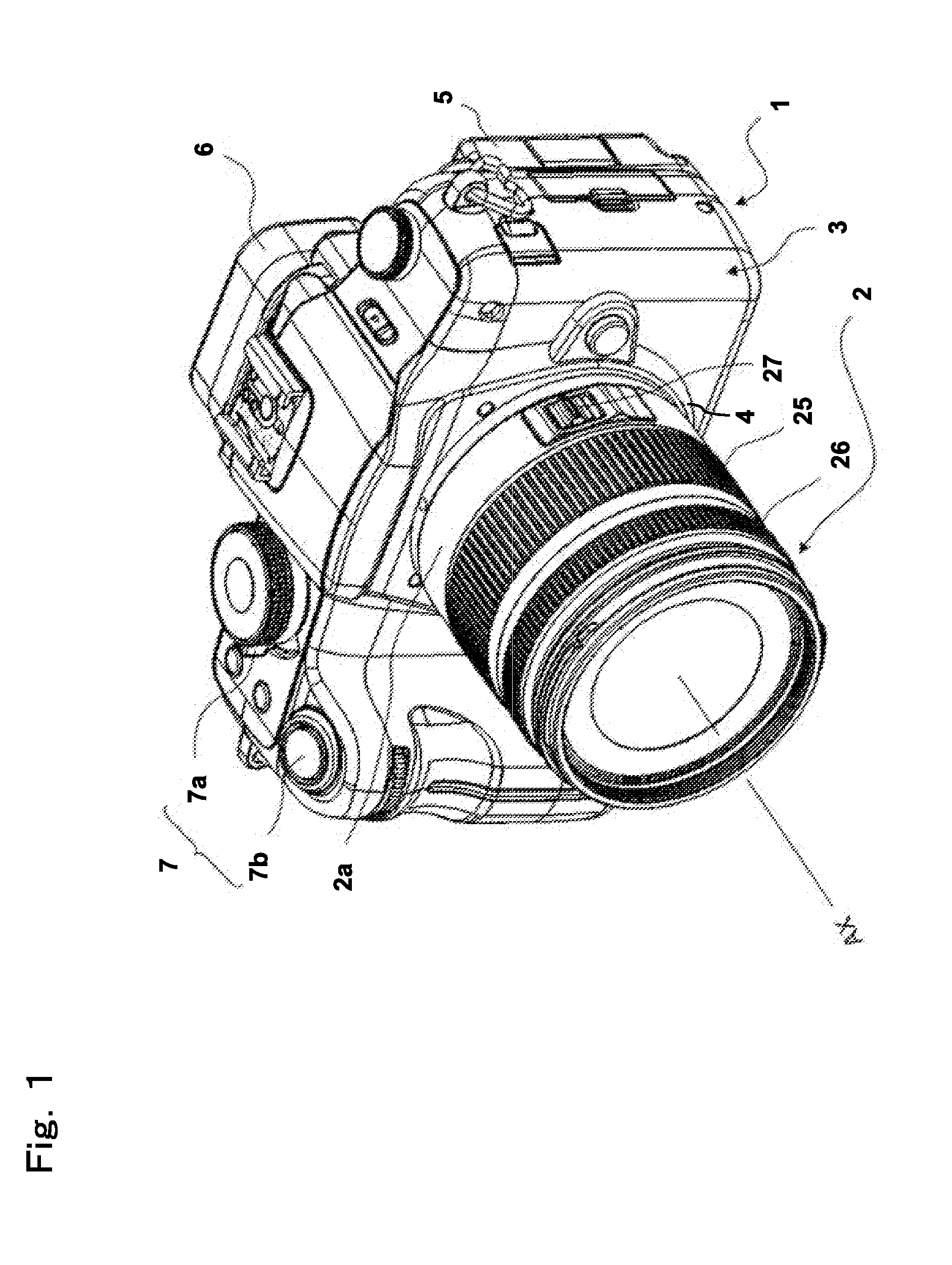
[0044]FIG. 1 is a perspective view of an outer appearance of a digital camera (which is an exemplary imaging device) according to a first embodiment of the present disclosure. The digital camera according to the first embodiment includes a camera main body 1 and an exchangeable lens unit 2 which is mountable to the camera main body 1. FIG. 2 is a perspective view of an outer appearance of the camera main body 1 from which the exchangeable lens unit 2 is removed. FIG. 3 is a schematic cross-sectional view of an internal structure of the digital camera. FIG. 4 is a functional block diagram illustrating the digital camera.

[0045]Firstly, referring to FIG. 1 to FIG. 4, a fundamental structure of the digital camera according to the first embodiment will be described. In the description herein, for convenience of description, an object side of the digital camera is referred to as the front, and an imaging plane side of the digital camera is referred to as the rear or the b...

Example

Second Embodiment

[0102]FIG. 12 is a cross-sectional view of an internal structure of an imaging device 200, as viewed from thereabove, according to a second embodiment of the present disclosure. For the present embodiment, control of a GND potential in the imaging sensor flexible cable and control of a GND potential in the metal plate will be mainly described, and detailed description of matters other than the controls is omitted. A fundamental structure of the imaging device 200 is the same as that of the digital camera described with reference to FIG. 1 to FIG. 4.

[0103]As shown in FIG. 12, the imaging device 200 includes the imaging sensor 110, the main circuit substrate 120, the imaging sensor flexible cable 130, the mount 140, the metal plate 150, the connection sections 160, electrically-conductive elastic sections 170, and the electrically-conductive section 190. The imaging sensor flexible cable 130 has GND exposure portions 132. The metal plate 150 has metal plate recesses ...

Example

Third Embodiment

[0116]FIG. 16 is a cross-sectional view of an internal structure of an imaging device 300, as viewed from thereabove, according to a third embodiment of the present disclosure. For the present embodiment, difference from the first embodiment will be mainly described. A fundamental structure of the imaging device 300 is the same as that of the digital camera described with reference to FIG. 1 to FIG. 4.

[0117]As shown in FIG. 16, the imaging device 300 includes the imaging sensor 110, the main circuit substrate 120, the imaging sensor flexible cable 130, the mount 140, the metal plate 150, the connection sections 160, and the electrically-conductive section 190. The imaging sensor flexible cable 130 has the GND exposure portions 131. The metal plate 150 has the metal plate projections 151. The main circuit substrate 120 has the GND removal portion 180 and the AD conversion LSI 185 (an integrated circuit for AD conversion) on the front surface on the metal plate 150 si...


PUM


Abstract

An imaging device includes: an imaging sensor 110; a main circuit substrate 120 includes a first ground conductor; an imaging sensor cable 130 that includes a second ground conductor, has the imaging sensor 110 mounted thereon, and is connected to the main circuit substrate 120; a metal plate 150 that is disposed between the main circuit substrate 120 and an area of the imaging sensor cable 130 where the imaging sensor 110 is mounted thereon, and that is electrically connected to the second ground conductor; and a ground connection conductor 190 that electrically connects between the first ground conductor and the metal plate 150. The ground connection conductor 190 is disposed in an area where the imaging sensor 110 and the imaging sensor cable 130 overlap each other or in an area where the imaging sensor 110 and the main circuit substrate 120 overlap each other.

Description

BACKGROUND[0001]1. Field[0002]The present disclosure relates to imaging devices such as digital still cameras and the like, and more particularly to imaging devices that allow image interference caused by an external noise to be reduced.[0003]2. Description of the Related Art[0004]In recent years, opportunities are increased in which imaging devices such as digital still cameras and the like are used in environments where portable information terminals, such as mobile telephones and PHSs (personal handyphone systems), which emit electromagnetic waves, are used. Further, there may be opportunities of imaging devices such as digital still cameras and the like being used in environments where intense electromagnetic waves are emitted, e.g. at or near a radio station or a television station.[0005]In a case where the imaging device is used in such an environment, the imaging device is likely to be subjected to an electromagnetic interference. Hereinafter, an environment in which imaging ...

Claims


Application Information

Patent Timeline
IPC IPC(8): H04N5/225
CPCH04N5/2253H04N2101/00H04N5/3577H04N23/54H04N25/617
Inventor TOBINAGA, MASATOFUSAYASU, HIROTSUGUKUMOI, MASAFUMINAGAOKA, RYUICHINISHIZAWA, YOSHIOINOUE, ATSUSHI
Owner PANASONIC INTELLECTUAL PROPERTY MANAGEMENT CO LTD
Why Eureka
Try Eureka