

Method for manufacturing a semiconductor device
- Summary
- Abstract
- Description
- Claims
- Application Information
AI Technical Summary
Benefits of technology
Problems solved by technology
Method used
Image

Examples
first embodiment
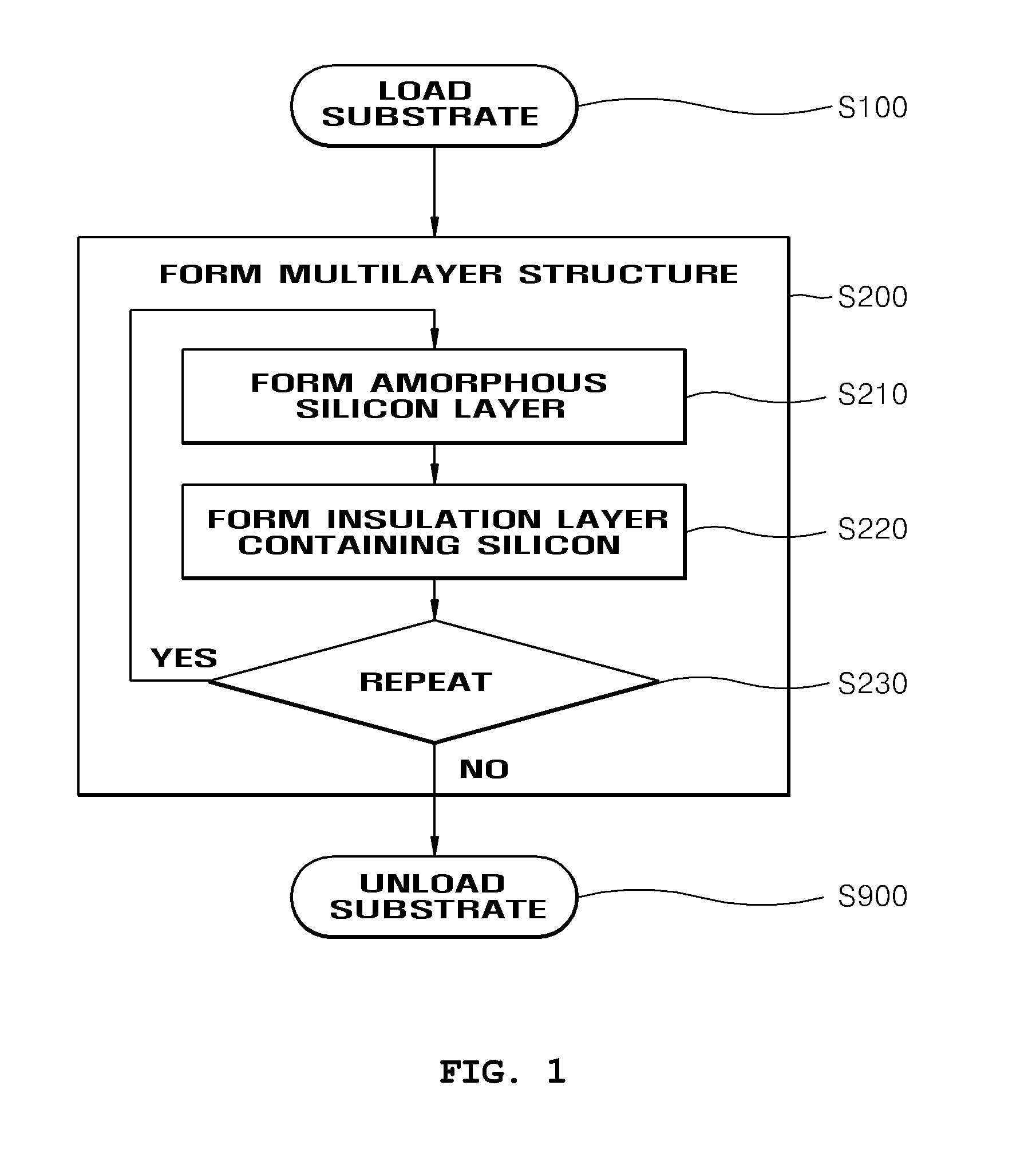
[0034]FIG. 1 is a flowchart illustrating a method of manufacturing a semiconductor device having a multilayer structure according to the present invention.
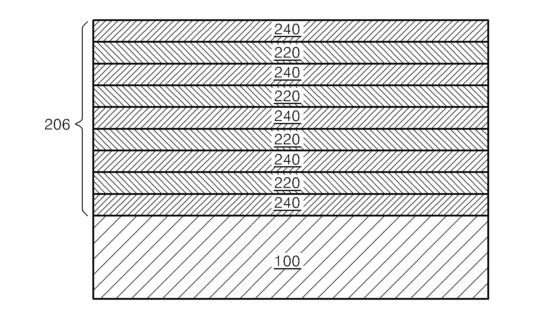
[0035]Referring to FIG. 1, a substrate is loaded into a chamber of a chemical vapor deposition (CVD) apparatus (S100). A multilayer structure may be formed on the substrate loaded into the chamber (S200). To form the multilayer structure, a process of forming an amorphous silicon layer (S210) and a process of forming an insulation layer containing silicon (S220) may be performed together with each other.
[0036]The amorphous silicon layer may be formed of doped conductive amorphous silicon. To form the amorphous silicon layer, a silicon-based gas that is a source gas may be used as a silicon precursor. Also, to form the amorphous silicon layer formed of the doped conductive amorphous silicon, a conductive dopant may be supplied together.
[0037]The insulation layer containing the silicon may be formed of silicon oxide or silicon nitri...
second embodiment
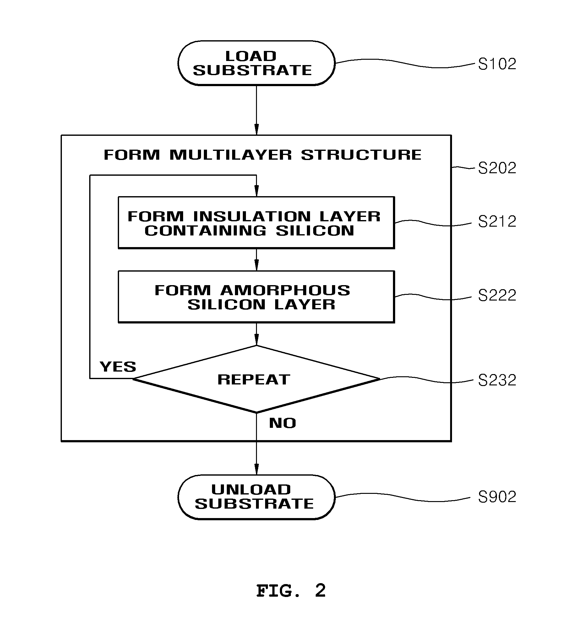
[0043]FIG. 2 is a flowchart illustrating a method of manufacturing a semiconductor device having a multilayer structure according to the present invention.
[0044]Referring to FIG. 2, a substrate is loaded into a chamber of a chemical vapor deposition (CVD) apparatus (S102). A multilayer structure may be formed on the substrate loaded into the chamber (S202). Here, a process of forming an insulation layer containing silicon (S212) and a process of forming an amorphous silicon layer (S222) may be performed together with each other to form the multilayer structure.
[0045]To form the multilayer structure, the process of forming the insulation layer containing the silicon (S212) and the process of forming the amorphous silicon layer (S222) may be repetitively performed (S232) in consideration of the number of layers of the multilayer structure to be formed. After the multilayer structure is formed, the substrate may be unloaded from the inside of the chamber of the CVD apparatus (S902).
[00...
PUM
 Abstract
Description
Claims
Application Information