Semiconductor Device and Manufacturing Method thereof

a technology of semiconductors and devices, applied in the direction of semiconductor devices, electrical devices, transistors, etc., can solve the problems of complex fabrication process, and achieve the effect of increasing the requirements of fin dimension and enhancing the carrier mobility of the devi

Active Publication Date: 2013-05-30
SEMICON MFG INT (SHANGHAI) CORP +1
View PDF0 Cites 13 Cited by
  • Summary
  • Abstract
  • Description
  • Claims
  • Application Information

AI Technical Summary

Benefits of technology

[0006]Generally, the increasing requirements on fin dimension c

Problems solved by technology

However, as the CMOS semiconductor device technology ad

Method used


Image

  • Semiconductor Device and Manufacturing Method thereof
  • Semiconductor Device and Manufacturing Method thereof
  • Semiconductor Device and Manufacturing Method thereof

Examples


Embodiment Construction

[0037]Hereinafter, embodiments of the present disclosure will be described with reference to the accompanying drawings.

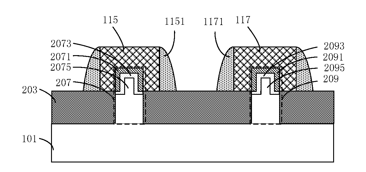
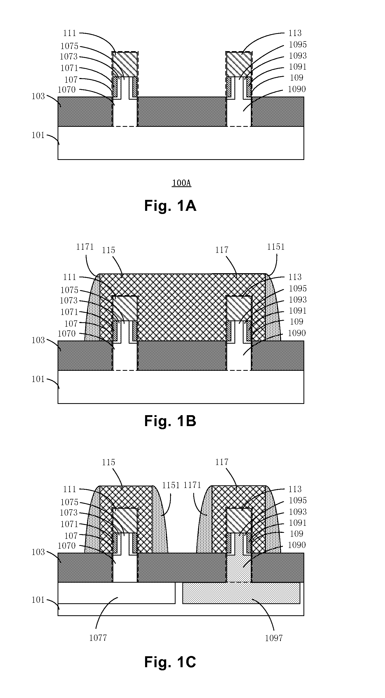
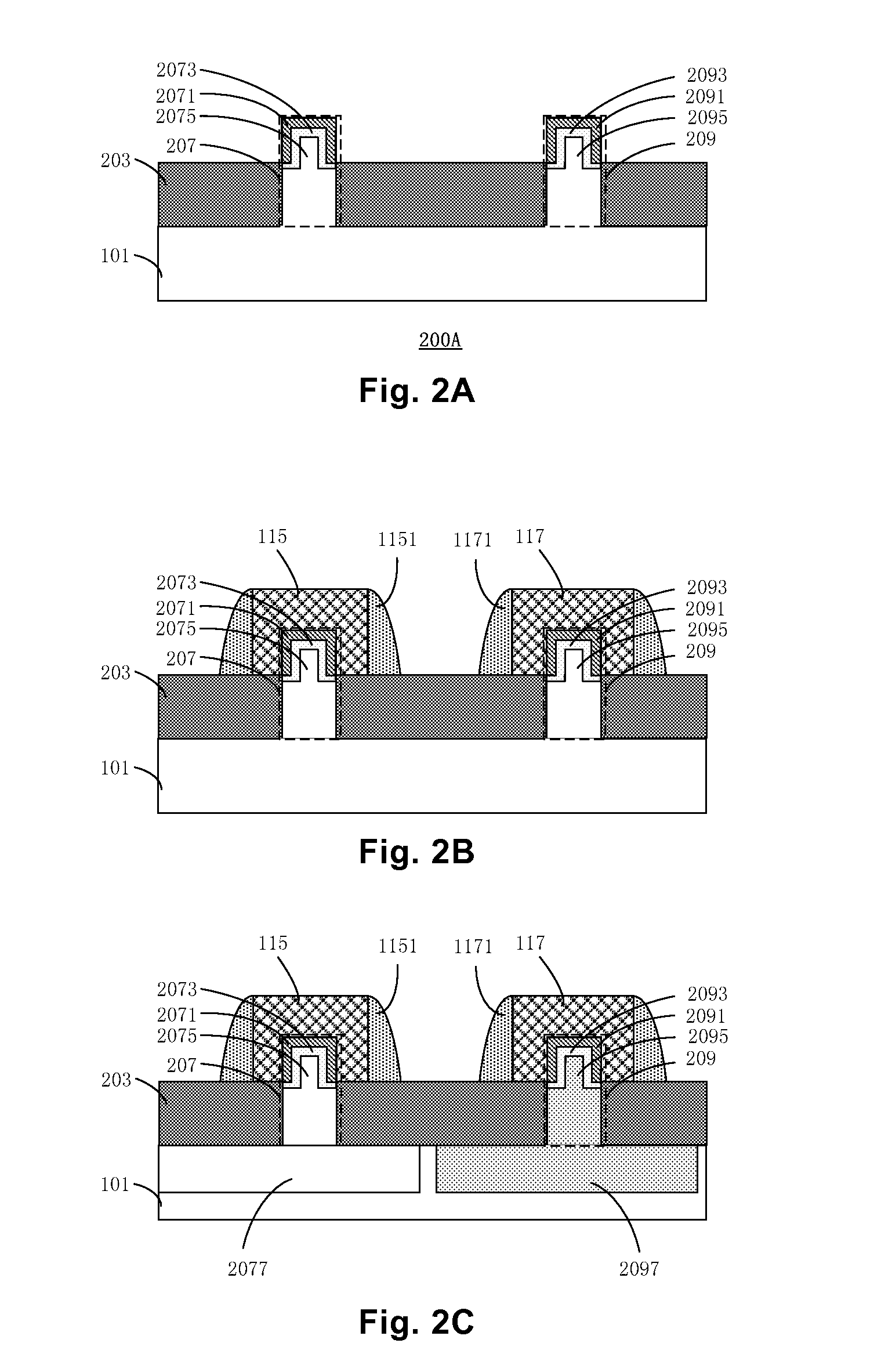
[0038]FIG. 1A shows a semiconductor device 100A according to one embodiment of the present disclosure. The semiconductor device 100A comprises a substrate 101 on which one or more fins (such as fins 107 and 109, as indicated in the dotted block of FIG. 1) are formed. Herein, in one embodiment, the substrate can be a bulk substrate, such as a bulk silicon substrate.

[0039]An insulating material layer (a first insulating material layer) 103 is also formed over the substrate 101 to surround the fins 107 and 109 so as to support the fins. In one embodiment, the insulating material layer 103 has a thickness that is less than the thickness of the fins. More preferably, a ratio of the thickness T of the insulating material layer 103 to the difference between the height Hsemi of the semiconductor layer 1070 / 1090 and the thickness T of the insulating material layer 103 is abo...


PUM


Abstract

A semiconductor device and a manufacturing method thereof are provided. The fin semiconductor device includes a fin formed on a substrate and an insulating material layer formed on the substrate and surrounding the fin. The fin has a semiconductor layer that has a source region portion and a drain region portion. The fin includes a first channel control region, a second channel control region, and a channel region between the two channel control regions, all of which are positioned between the source region portion and the drain region portion. The two channel control regions may have the same conductivity type, different from the channel region.

Description

CROSS-REFERENCE TO RELATED APPLICATIONS[0001]This application claims priority to Chinese Patent Application No. CN201110377035.3 filed on Nov. 24, 2011 and entitled “Semiconductor Device and Manufacturing Method Thereof”, which is incorporated herein by reference in its entirety.FIELD OF THE INVENTION[0002]The present invention relates to the field of semiconductor technology, and more specifically, relates to a semiconductor device and a manufacturing method thereof.DESCRIPTION OF THE RELATED ART[0003]With continuous development of semiconductor technology, critical dimensions of a device are continuously shrinking. Under such trend, a MOS semiconductor device, such as a CMOS transistor, has been proposed.[0004]However, as the CMOS semiconductor device technology advances, the fabrication process has become more complex. Thus, FinFET gradually becomes a desirable alternative for MOSFET because of its simple fabrication process.[0005]There exists a need for fin JFET as well as manuf...

Claims


Application Information

Patent Timeline
IPC IPC(8): H01L29/78H01L21/336
CPCH01L27/098H01L29/785H01L29/66901H01L21/26586H01L29/0657H01L21/823821H01L27/0924H01L29/808
Inventor FUMITAKE, MIENO
Owner SEMICON MFG INT (SHANGHAI) CORP
Why Eureka
Try Eureka