

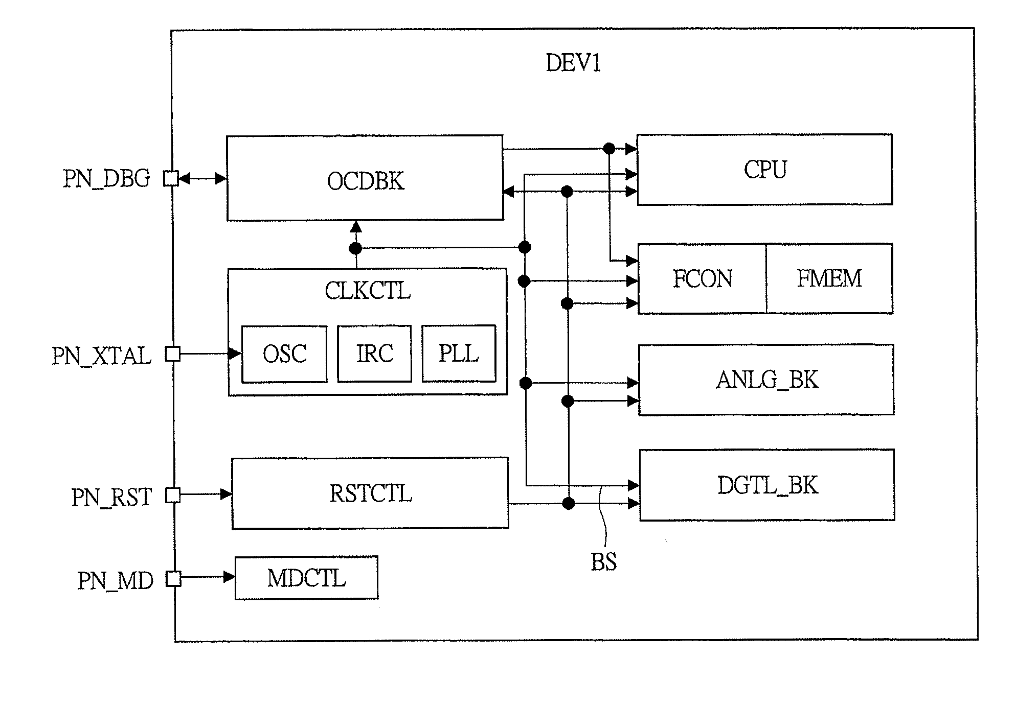
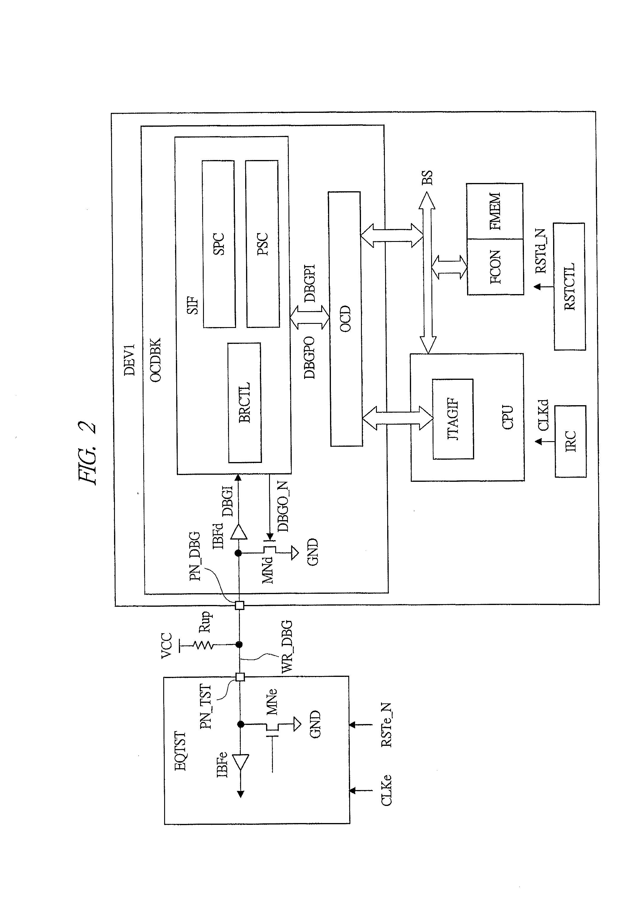
Electronic Apparatus
a technology of electronic equipment and circuits, applied in the direction of transmission monitoring, memory adressing/allocation/relocation, instruments, etc., can solve the problems of incorrect initial transmitting and receiving processes of baud rate setting commands, and the circuit area (costs) of the ic chip (as well as the electronic apparatus) might increase. , to achieve the effect of increasing the circuit area (costs) of the ic chip
- Summary
- Abstract
- Description
- Claims
- Application Information
AI Technical Summary
Benefits of technology
Problems solved by technology
Method used
Image

Examples
modification examples
Various Modification Examples
Operation of Baud Rate Adjusting Circuit
[0111]In the above descriptions, the baud rate calculation has been carried out by using the average value of the total 9 bits including the start bit (1 bit) STR, and succeeding data bits (8 bits) DAT, as illustrated in FIG. 6 etc.; however, although not particularly limited by this, any average value of a total of 2 bits or more may be used. For example, in the case when an average value of the STR of 1 bit and the succeeding DAT of 7 bits, that is, 8 bits, is used, since its dividing process can be realized by a shift resister or the like, the easiness of the dividing process, the reduction in the area of the dividing circuit, etc. can be achieved in comparison with a case using 9 bits in total. From this point of view, 4 bits in total, 2 bits in total, or the like, may be used. In this case, however, as the number of bits increases, the detection precision of baud rate can be improved; therefore, in particular,...
PUM
 Abstract
Description
Claims
Application Information