Liquid Crystal Display Device Having Discharge Circuit And Method Of Driving Thereof

Active Publication Date: 2013-06-13
LG DISPLAY CO LTD
View PDF5 Cites 24 Cited by
  • Summary
  • Abstract
  • Description
  • Claims
  • Application Information

AI Technical Summary

Benefits of technology

[0038]According to a liquid crystal display device having the foregoing configuration and a method of driving the same associated with at least one embodiment of the present invention, residual charge flowing from the liquid crystal display panel to the gate driving unit when turning on the liquid crystal display

Problems solved by technology

Furthermore, the liquid crystal display device may include a backlight unit for supplying light to the liquid crystal display device because it is unable to spon

Method used


Image

  • Liquid Crystal Display Device Having Discharge Circuit And Method Of Driving Thereof
  • Liquid Crystal Display Device Having Discharge Circuit And Method Of Driving Thereof
  • Liquid Crystal Display Device Having Discharge Circuit And Method Of Driving Thereof

Examples


Example

[0069]FIG. 3 is a block diagram illustrating a gate driving unit according to a first embodiment of the present invention, and FIG. 4 is a block diagram illustrating a level shifter and a discharge circuit according to a first embodiment of the present invention.

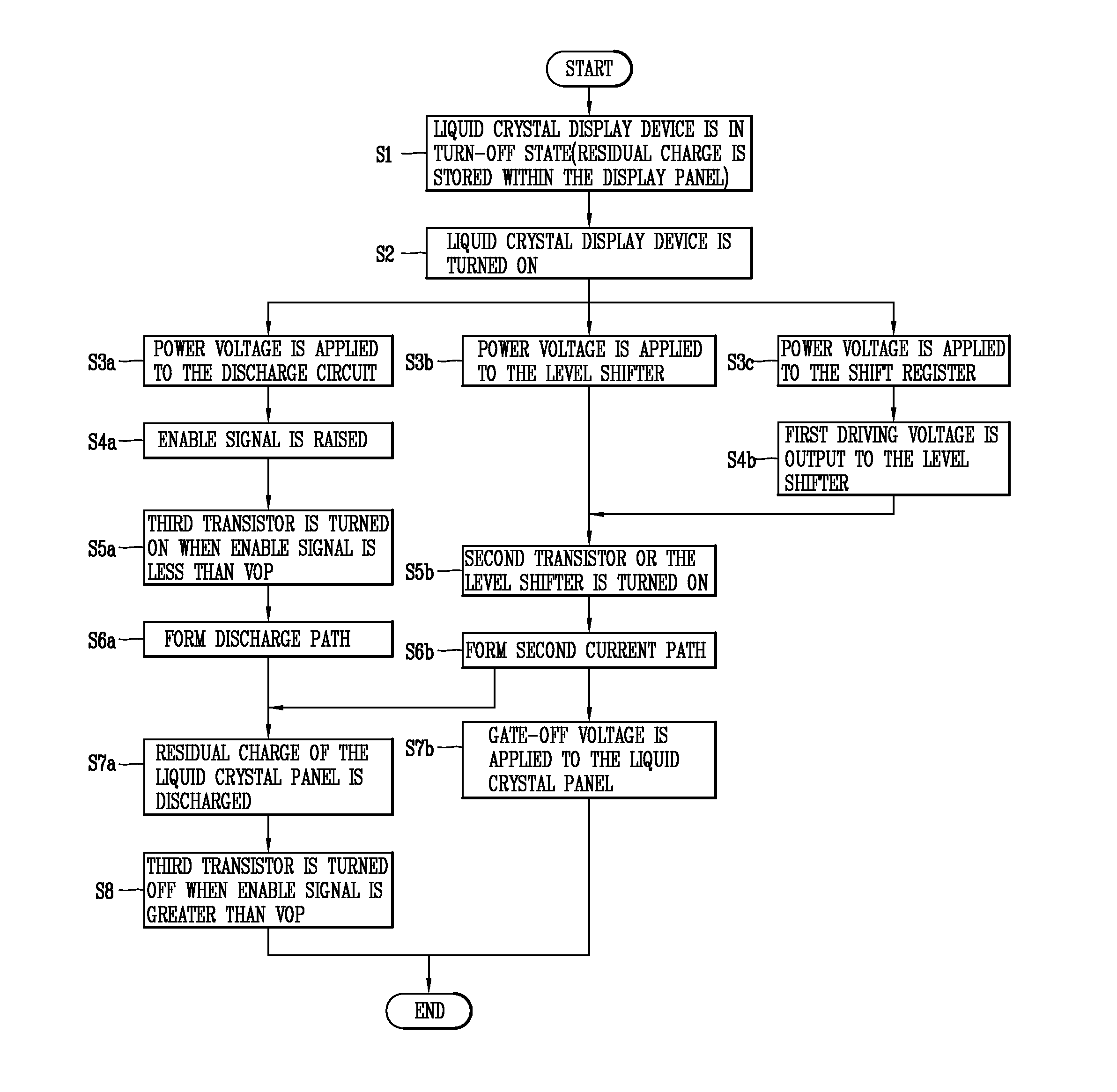
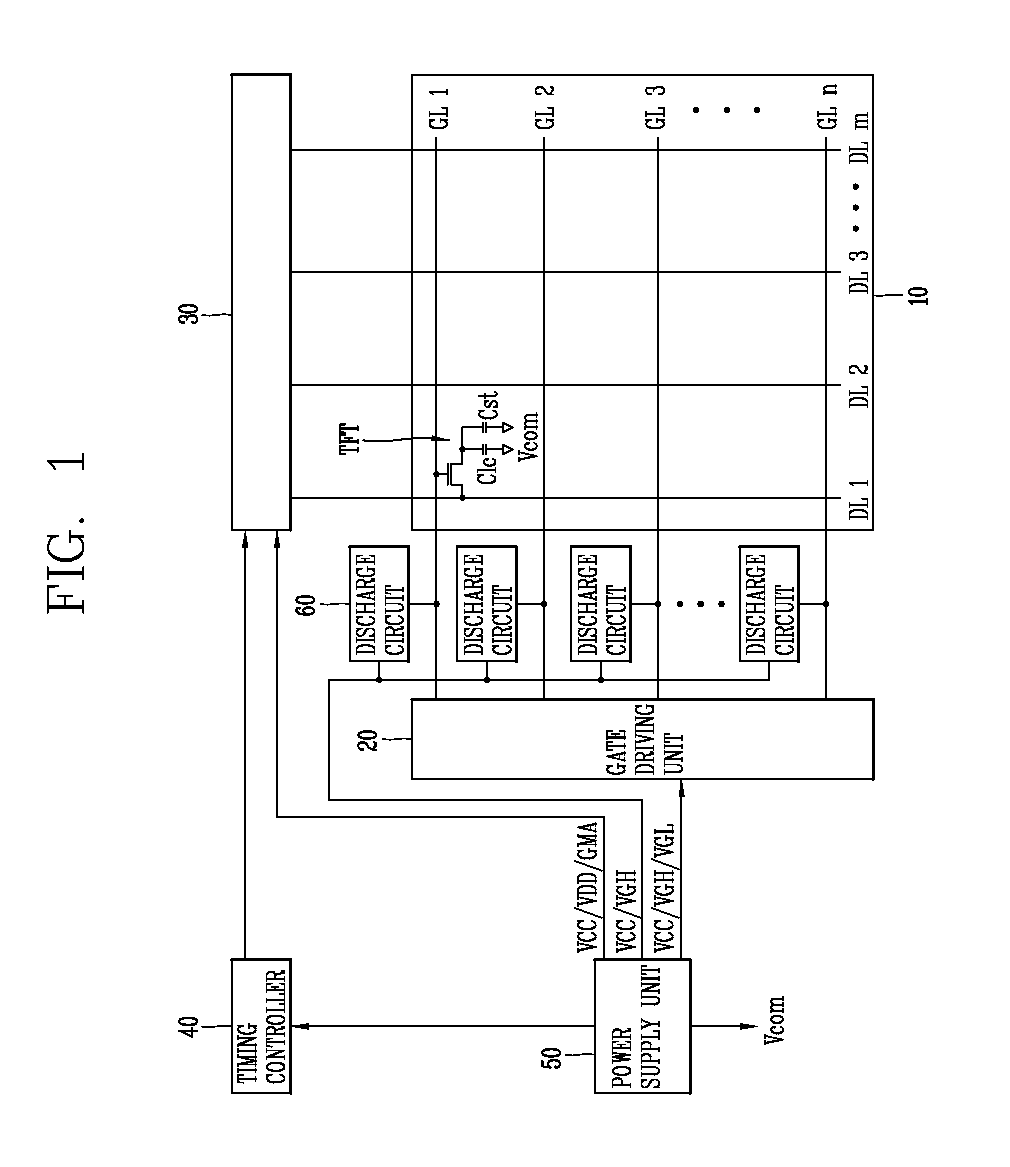
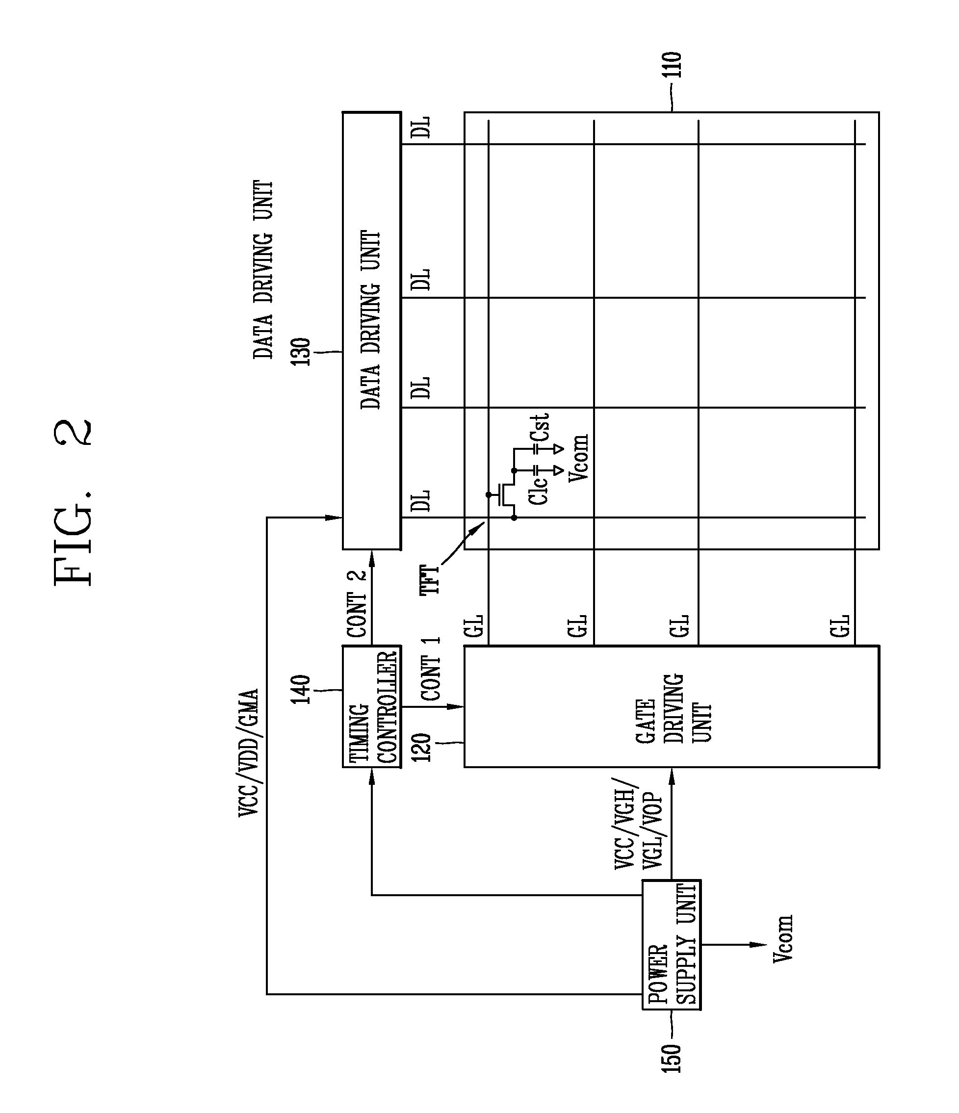
[0070]The gate driving unit according to a first embodiment of the present invention may include a shift register 121, a level shifter 122, an output buffer unit 123, and a discharge circuit 124.

[0071]The shift register 121 receives a plurality of gate shift clock signals (GSCs) and a gate start pulses (GSP) among the gate control signals (CONT1) to shift the gate start pulse (GSP), thereby outputting a sequentially shifted gate driving voltage (SO). The gate driving voltage (SO) may include a first driving voltage at a high level and a second driving voltage at a low level.

[0072]The level shifter 122 enhances the swing voltage of the gate driving voltage (SO) to supply the gate voltage (LO) to each of the gate lines.

[0073]T...

Example

[0111]Hereinafter, a discharge circuit according to a second embodiment of the present invention will be described in detail.

[0112]FIG. 8 is a circuit diagram illustrating the discharge circuit and level shifter according to a second embodiment of the present invention. A liquid crystal display device according to a second embodiment of the present invention does not include an auxiliary discharge circuit, and the remaining configuration thereof is the same as that of the first embodiment of the present invention, and the description thereof is substituted by the description of the first embodiment.

[0113]The level shifter 222 according to a second embodiment of the present invention may include a first transistor (T11), a second transistor (T12), and a first diode (D 11). Similar to the first embodiment, the first transistor (T11) may form a first current path in which the gate-on voltage (VGH) is applied to the liquid crystal display panel, and the second transistor (T12) may form ...


PUM


Abstract

A liquid crystal display device discharges residual charge within the liquid crystal display panel. The liquid crystal display device comprises pixels defined by gate lines and data lines intersecting with each other and switching elements for driving the plurality of pixels; a level shifter comprising a first transistor connected between a gate-on voltage terminal and an output terminal and a second transistor connected between a gate-off voltage terminal and the output terminal to selectively output either the gate-on voltage or gate-off voltage to the plurality of gate lines; and a discharge circuit forming a discharge path connecting the gate-off voltage terminal and the ground terminal. The second transistor is turned on during the power-on of the liquid crystal display panel to apply the gate-off voltage. The discharge circuit is turned on to discharge the residual charge of the liquid crystal display panel through the discharge path.

Description

CROSS-REFERENCE TO RELATED APPLICATIONS[0001]This application claims the benefit of Korean Patent Application No. 10-2011-0133685, filed on Dec. 13, 2011, which is hereby incorporated by reference for all purposes as if fully set forth herein.BACKGROUND OF THE INVENTION[0002]1. Field of the Invention[0003]The present invention relates to a liquid crystal display device and method of driving the same, and more particularly, to a liquid crystal display device and method of driving the same for removing the effect of residual charge when turning on the liquid crystal display panel.[0004]2. Description of the Related Art[0005]In general, a liquid crystal display device is a display device for generating image information to pixels arranged in a matrix form, and adjusting the optical transmittance of the pixels to display desired images. Accordingly, the liquid crystal display device may include a liquid crystal display panel in which pixels (i.e., the minimum units for displaying an ima...

Claims


Application Information

Patent Timeline
IPC IPC(8): G02F1/1362G09G3/36G02F1/1368
CPCG02F1/136204G02F1/1368G09G3/36G09G2330/04G09G3/3674G09G2310/0245G09G3/3648G02F1/133
Inventor SUNG, CHANGYONGMOON, SUNGJOONKIM, SEYEONCHOI, SEONGHUN
Owner LG DISPLAY CO LTD
Why Eureka
Try Eureka