Device having spad photodiodes for detecting an object

Active Publication Date: 2013-06-20
STMICROELECTRONICS (GRENOBLE 2) SAS
View PDF1 Cites 64 Cited by
  • Summary
  • Abstract
  • Description
  • Claims
  • Application Information

AI Technical Summary

Benefits of technology

[0009]One embodiment avoids this limitation induced by the high voltage generation circuit, and provides the detection circuit with a sufficient number of SPAD photodiodes, giv

Problems solved by technology

The result is that the more photodiodes in the circuit, the greater the surface occupied by the

Method used


Image

  • Device having spad photodiodes for detecting an object
  • Device having spad photodiodes for detecting an object
  • Device having spad photodiodes for detecting an object

Examples


Embodiment Construction

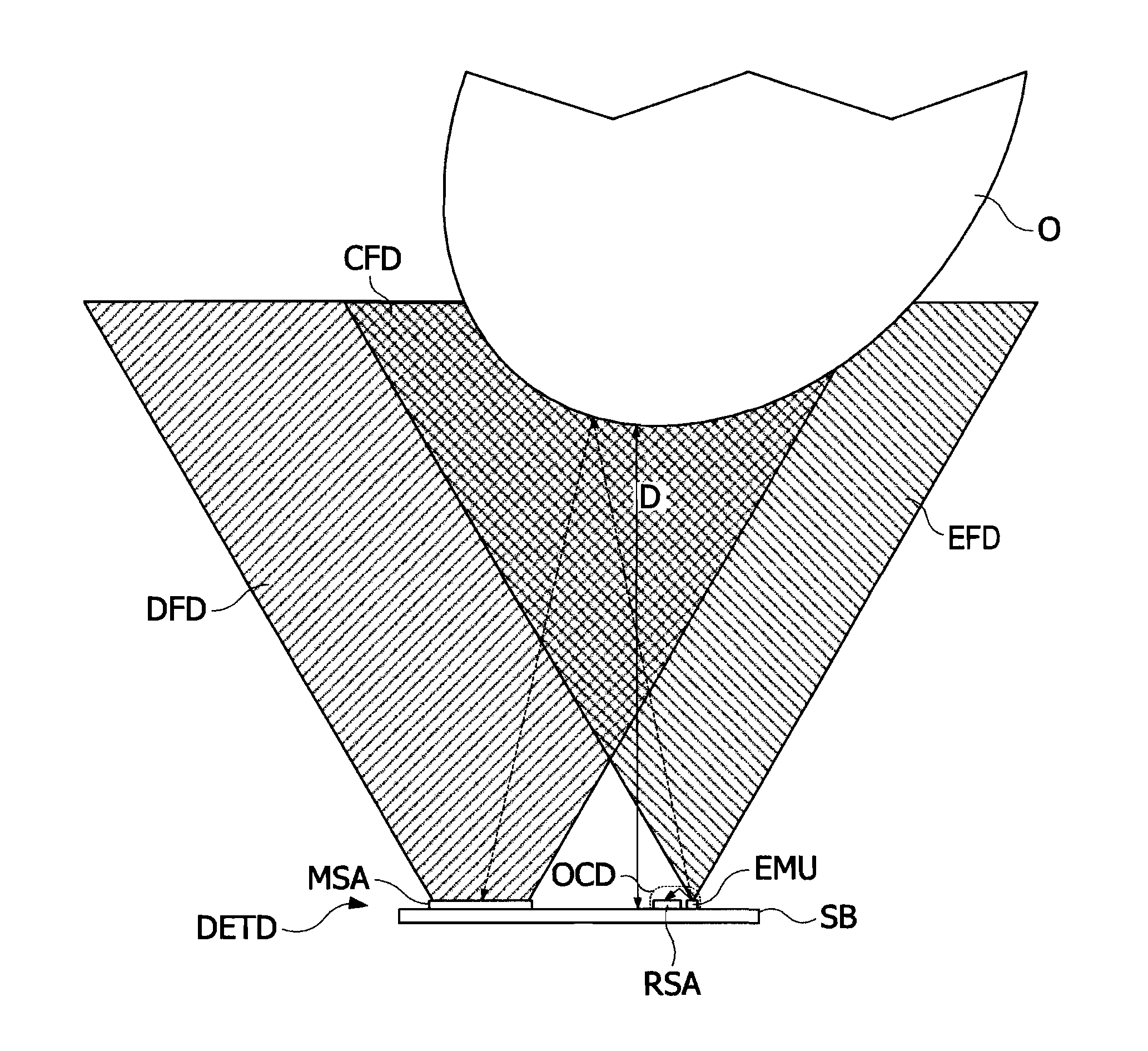
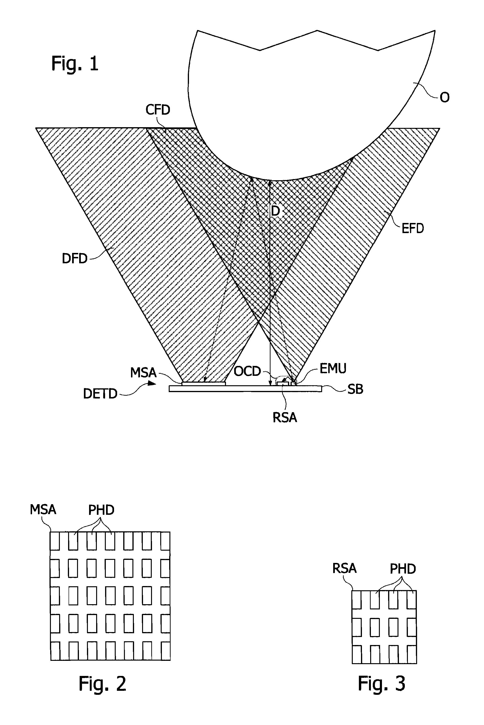
[0035]FIG. 1 shows a detection device DETD, according to one embodiment. Detection device DETD comprises a light emission unit EMU emitting photon pulses, a reception unit MSA, and a reference reception unit RSA. The reception unit MSA and the reference reception unit RSA are sensitive to the photon pulses emitted by the light emission unit EMU. The light emission unit EMU, the reception unit MSA, and the reference reception unit RSA are formed on a wafer SB for example in a semiconductor material. The light emission unit EMU emits photon pulses in an emission field EFD for example of conical shape whose top is centered on light emission unit EMU. The reception unit MSA is sensitive to photons coming from a detection field DFD which may also be of conical shape. Fields EFD and DFD have a common area, forming a common detection field CFD in which an object O may be detected by detection device DETD by reflecting photons emitted by light emission unit EMU toward reception unit MSA.

[00...


PUM


Abstract

The disclosure relates to a method for detecting the presence of an object near a detection device, comprising: reverse biasing single photon avalanche photodiodes, at a bias voltage greater than a breakdown voltage of a PN junction of each photodiode, emitting pulses of an incident photon beam, detecting photodiodes which avalanche trigger after the reception by the photodiode of at least one photon of a reflected photon beam produced by a reflection of the incident beam on an object near the detection device, determining the object presence as a function of the existence of at least one avalanche triggering in one of the photodiodes, and selecting a number of photodiodes to be reverse biased in relation to the detection device, as a function of a load of a circuit for generating the bias voltage.

Description

BACKGROUND[0001]1. Technical Field[0002]The present disclosure relates to a device for detecting and measuring the distance to an object, based on a propagation time of a photon beam emitted in the form of pulses and reflected on the object. The present disclosure applies in particular to touch screens such as those used in mobile phones, and to the detection of an object near such a screen.[0003]2. Description of the Related Art[0004]It is known to use photodiodes as a distance detection and measurement element, using an avalanche phenomenon which may occur in the PN junctions of photodiodes. An avalanche phenomenon may occur in a diode PN junction when the diode is reverse biased near the junction breakdown voltage. This phenomenon can be used in two ways in an avalanche photodiode. If the avalanche photodiode is reverse biased just below the breakdown voltage, the photodiode then generates an electric current proportional to the intensity of the photon flux received by the photod...

Claims


Application Information

Patent Timeline
IPC IPC(8): G01J1/02G01S7/486G01S17/04G01S17/18G01S17/89
CPCG01S17/026G01S17/107G01S17/89G01S7/4814G01J1/02G01S7/484G01S7/486G01S7/489G01S7/4816G01S17/04G01S17/18
Inventor DRADER, MARCMELLOT, PASCAL
Owner STMICROELECTRONICS (GRENOBLE 2) SAS
Why Eureka
Try Eureka