Charge pump circuit for high voltage generation

a pump circuit and high voltage technology, applied in the field of capacitor voltage multiplier circuits, can solve the problems of limiting the voltage gain achieved at each pump stage, severely degrading the pumping efficiency of the multiplier, and reducing the output gain of boosting voltage to an unusable condition, etc., to achieve simple and quite regular layout, reduce transfer losses, and simplify the production of high voltage multiplier circuits

Active Publication Date: 2008-07-24
ETRON TECH INC
View PDF10 Cites 49 Cited by
  • Summary
  • Abstract
  • Description
  • Claims
  • Application Information

AI Technical Summary

Benefits of technology

[0024]A principal object of the present invention is to realize a circuit for voltage multiplier applications implementing a Charge Pump (CP) Circuit for High Voltage Generation exhibiting low power consumption and at the same time high conversion efficiency values.
[0025]Another principal object of the present invention is to provide an effective and very manufacturable method for implementing a circuit for voltage multipliers as an integrated circuit (IC) for high positive as well as negative output voltages.

Problems solved by technology

These have to be considered however in more detail because it is well known that voltage multiplier circuits based on Dickson's architecture fail to provide sufficient pumping efficiency when the power supply voltage VDD becomes very low, in which case their output gains for boosting voltages decrease to an unusable condition.
As already mentioned, this will severely degrade the pumping efficiency of the multiplier.
However, the amplitude VBST of clock pulses BSTA and BSTB, pump capacitance (C) of capacitors C1, C2, and C3, parasitic stray capacitance (Cs), and load current are factors that can limit the voltage gain achieved at each pump stage.
Five major drawbacks shall be listed in the following:First, its charge sharing process is not completely executed, which is owed to the threshold voltage of the diode connected MOS transistor, i.e. there is always one forward diode drop voltage difference between two adjacent charge sharing nodes, which thus reduces efficiency.
The more CP-stages are connected in series the less pumping efficiency is obtained, or in other words, extra stages are required to reach said certain target voltage due to this lowered efficiency.Third, owed to the body effect the threshold voltage of higher order CP-stage's will gradually increase.
In other words, when it comes to low supply voltage levels the circuit does not perform well.Fourth, the charge sharing speed is rather slow because the diode-configured NMOS transistors are always working in saturation region.
This will increase the charge sharing time and also reduce the magnitude of the pump current within the CP because the value of the CP's settlement current is reciprocal to the charge sharing time, i.e. the time during which two capacitors are connected together.Fifth, the breakdown voltage of the diode connected MOS transistors must increase as CP output voltage increases, which signifies that the higher order MOS transistors oxide stress is gradually increased, which will decrease the rise time of the pumping circuit and also degrade reliability.
Moreover, such voltage generator circuits also may consume a significant amount of power relative to the remainder of the circuit, and thus increase the current that must be supplied by the user (e.g. by the VDD power supply).
Consequently the unwanted increase in power dissipation increases the temperature of the die during operation.
In a battery-powered environment, any increase in power consumed by a device has significant implications for battery life, and any additional heat generated is also more difficult to dissipate.
It is therefore a challenge for the designer of such circuits to achieve a higher efficiency solution.
However these approaches use often solutions, which are somewhat technically complex and therefore also expensive in production.

Method used


Image

  • Charge pump circuit for high voltage generation
  • Charge pump circuit for high voltage generation
  • Charge pump circuit for high voltage generation

Examples


Embodiment Construction

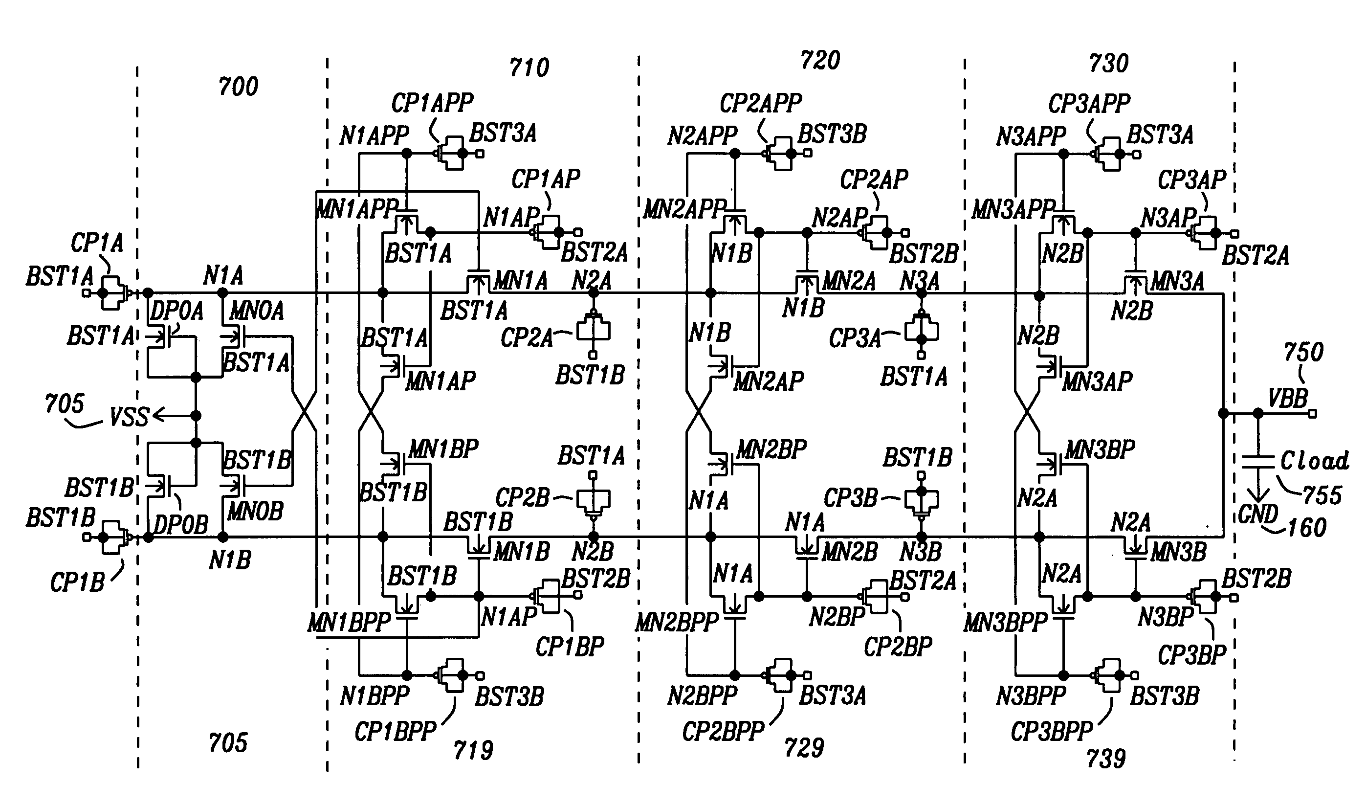
[0069]The preferred embodiments disclose novel realizations for “A New Charge Pump Circuit for High Voltage Generation” also known as voltage multiplier circuits. These circuits do exist as prior art in numerous variants but all have well-known sometimes significant drawbacks as already listed above. The technical approach for achieving the goal of avoiding most of the disadvantages is to make use of intelligent charge transfer switching (CTS) techniques i.e. replace diode connected MOSFETs by switching MOSFET structures, additionally substitute simpler anti-phase control schemes by more sophisticated multiphase control schemes in order to avoid losses during charge transfer transactions and last not least make use of an advanced technology for manufacturing the new circuits in integrated circuit implementation e.g. realizing crucial internal circuit parts of the chip as triple-well MOSFET structures. Using the intrinsic advantages of that solution—as described later on in every det...


PUM


Abstract

A circuit and method are given, to realize a high efficiency voltage multiplier for integrated circuits generating an internal and flexible positive or negative high voltage on-chip supply voltage from low external positive or negative supply voltages or ground. Applying multi-phase control signals to voltage boost internal nodes allows for eliminating threshold voltage drop losses and thus improves the voltage pumping gain compared to circuits with diode-configured FETs of prior art. Making use of voltage signals from antecedent stages in order to bias the bulk of MOS transistors fabricated in triple-well technology enables relaxing of the gate oxide stress within high order stage MOS transistors. Such a method, called leap-frog bulk potential tracking method, makes MOS transistors from different stages exhibit about the same body effect, which is very important because MOS transistors of higher order stages now show the same performance as MOS transistors from lower order stages. Important also in terms of efficiency as the charge sharing speed of high order MOS transistors always dominates the total charge pump performance and the driving force of pumped currents, thus also allowing for a greater number of serially connectable stages overall or a smaller number necessary for a certain targeted output voltage.

Description

BACKGROUND OF THE INVENTION[0001](1) Field of the Invention[0002]The present invention relates in general to semiconductor voltage generator circuits, and particularly to capacitive voltage multiplier circuits using MOS transistors, even more particularly to voltage multiplier circuits using charge pumps manufactured as semiconductor integrated circuits.[0003](2) Description of the Prior Art[0004]Recent developments in electronic devices for modern mobile and portable equipment for telecommunications and data processing have strengthened a tendency to an ever-continuing decrease of the applied supply voltages and furthermore to prefer components still needing one single supply voltage only. Portable devices are in general powered by batteries and weight and size of modern batteries play an important role in customer's acceptance, thus smaller devices with small batteries however furnishing low voltages only are in focus of current manufacturing and marketing strategies. Most modern ...

Claims


Application Information

Patent Timeline
Patent Type & Authority Applications(United States)
IPC IPC(8): G05F3/02
CPCH02M2003/077H02M3/073H02M3/077
Inventor HSU, JEN-SHOU
Owner ETRON TECH INC
Why Eureka
Try Eureka