Method and apparatus for analyzing and/or repairing of an EUV mask defect

a technology of euv mask and defect analysis, applied in the field of analyzing and/or repairing of euv mask defect, can solve problems such as phase errors and amplitude errors

Active Publication Date: 2013-06-20
CARL ZEISS SMT GMBH
View PDF3 Cites 23 Cited by
  • Summary
  • Abstract
  • Description
  • Claims
  • Application Information

AI Technical Summary

Benefits of technology

[0031]In a further aspect determining the optimal repairing method comprises selecting one of the different repairing methods as the optimal repairing method which generates a focus stack which maximizes a process window for the EUV optical element at the illumination of a wafer.
[0032]The process window is maximized for the repairing method whose aerial images of the focus stack fulfill a

Problems solved by technology

The described method exploits that amplitude errors and phas

Method used


Image

  • Method and apparatus for analyzing and/or repairing of an EUV mask defect
  • Method and apparatus for analyzing and/or repairing of an EUV mask defect
  • Method and apparatus for analyzing and/or repairing of an EUV mask defect

Examples


Embodiment Construction

[0084]In the following, the present invention will be more fully described with reference to the accompanying figures, in which exemplary embodiments of the invention are illustrated. However, the present invention may be embodied in different forms and should not be construed as limited to the examples set forth herein. Rather, these examples are provided so that the disclosure will be thorough and will convey the scope of the invention to persons skilled in the art.

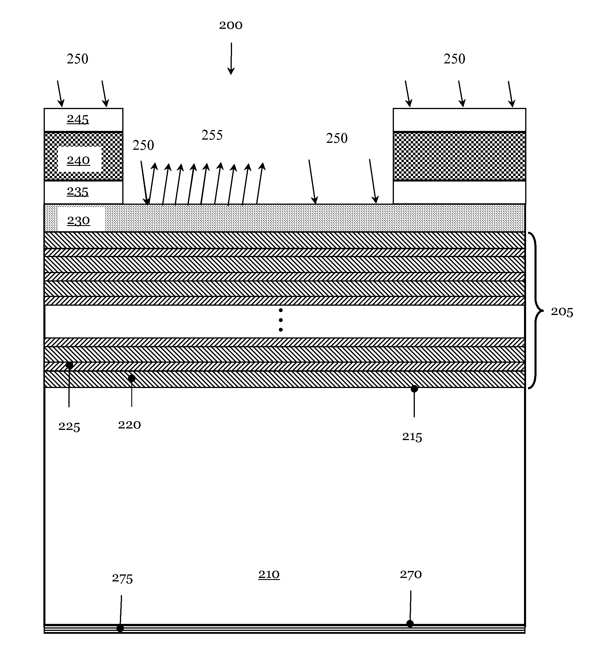
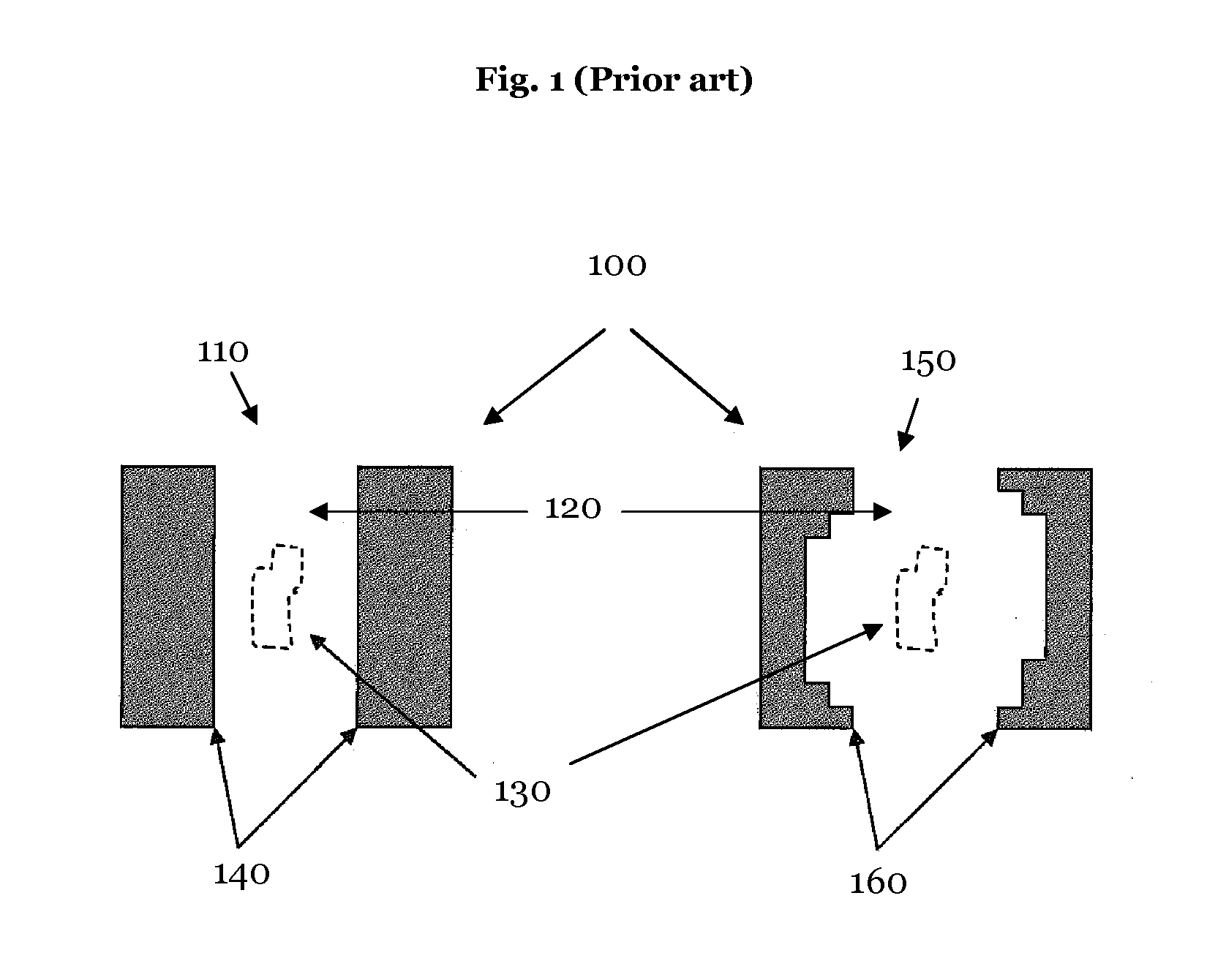
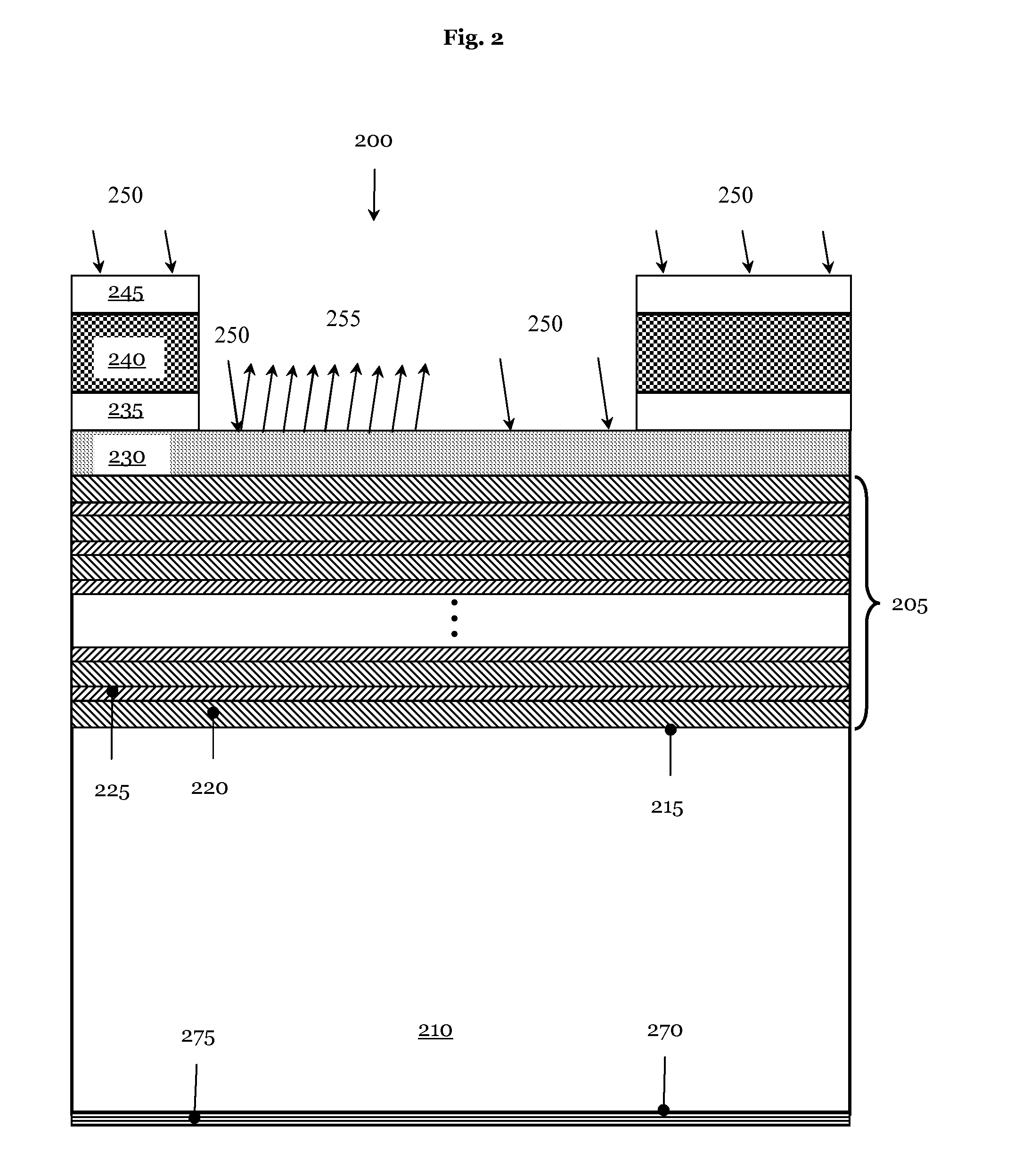
[0085]FIG. 1 shows a top view of a cut-out of an EUV mask 100. The left diagram no comprises a multilayer structure 120 which has a multilayer defect 130 buried in the multilayer structure 120, which is called a buried defect. On the multilayer 120 two pattern elements 140 are arranged having a form of absorbing stripes. The right diagram 150 illustrates the absorber structure 160 of the left diagram no of the EUV mask 100 after the multilayer defect 130 of has been partially compensated by removing a portion of the abs...


PUM

PropertyMeasurementUnit
Energyaaaaaaaaaa
Energyaaaaaaaaaa
Energyaaaaaaaaaa

Abstract

The invention relates to a method for analyzing a defect of a photolithographic mask for an extreme ultraviolet (EUV) wavelength range (EUV mask) comprising the steps of: (a) generating at least one focus stack relating to the defect using an EUV mask inspection tool, (b) determining a surface configuration of the EUV mask at a position of the defect, (c) providing model structures having the determined surface configuration which have different phase errors and generating the respective focus stacks, and (d) determining a three dimensional error structure of the EUV mask defect by comparing the at least one generated focus stack of the defect and the generated focus stacks of the model structures.

Description

FIELD OF THE INVENTION[0001]The present invention relates to the field of analyzing and / or repairing of an EUV mask defect.BACKGROUND OF THE INVENTION[0002]As a result of the shrinking sizes of integrated circuits, photolithographic masks have to project smaller and smaller structures onto a photosensitive layer i.e. a photoresist dispensed on a wafer. In order to enable the decrease of the critical dimension (CD) of the structure elements forming the integrated circuits (ICs), the exposure wavelength of photolithographic masks has been shifted from the near ultraviolet across the mean ultraviolet into the far ultraviolet region of the electromagnetic spectrum. Presently, a wavelength of 193 nm is typically used for the exposure of the photoresist on wafers. As a consequence, the manufacturing of photolithographic masks with increasing resolution is becoming more and more complex.[0003]In the future, photolithographic masks will use even smaller wavelengths in the extreme ultraviole...

Claims


Application Information

Patent Timeline
IPC IPC(8): G01N21/95G06F17/50G03B27/68G06T7/00C23C14/48G21K5/00G03F1/24G03F1/72G03F1/74G03F1/84
CPCB82Y10/00B82Y40/00G03F1/24G03F1/72G03F1/74G03F1/84G21K5/00G03F7/7065C23C14/48G01N21/95G03B27/68G06F17/5009G06T7/0002G03F7/705G03F1/22G03F1/68G06F30/20
Inventor BUDACH, MICHAELBRET, TRISTANEDINGER, KLAUSHOFMANN, THORSTENFELDMANN, HEIKORUOFF, JOHANNES
Owner CARL ZEISS SMT GMBH
Why Eureka
Try Eureka