
Etching composition and method for fabricating semiconductor device using the same

a technology of etching composition and semiconductor devices, which is applied in the direction of semiconductor devices, electrical equipment, chemistry apparatus and processes, etc., can solve the problems of phosphoric acid, corrosive, and failure of the nitride film etching process, and achieve the effects of reducing the etching process difficulty

Active Publication Date: 2013-06-20
SK HYNIX INC
View PDF1 Cites 21 Cited by
  • Summary
  • Abstract
  • Description
  • Claims
  • Application Information

AI Technical Summary

Benefits of technology

This patent is about a special chemical that can remove nitride films without getting into oxide films. It also doesn't create any particles that can damage semiconductor devices. This chemical can be used to make semiconductor devices more efficiently.

Problems solved by technology

However, even when the amount of deionized water changes minutely, a failure occurs in the nitride film etching process.
Phosphoric acid, one of strong acids, is corrosive, and thus difficult to handle.
In an attempt to solve these problems, a technology of removing a nitride film using an etching composition comprising hydrofluoric acid (HF) and phosphoric acid (H3PO4) or nitric acid (HNO3) and phosphoric acid (H3PO4) was suggested, but resulted in a decrease in the etching selectivity for a nitride film with respect to an oxide film.
In addition, a technology of removing a nitride film using an etching composition comprising phosphoric acid and silicate or phosphoric acid and silicic acid was also suggested, but silicate or silicic acid is not suitable for use in semiconductor fabrication processes, because it causes generation of particles that may affect a substrate.
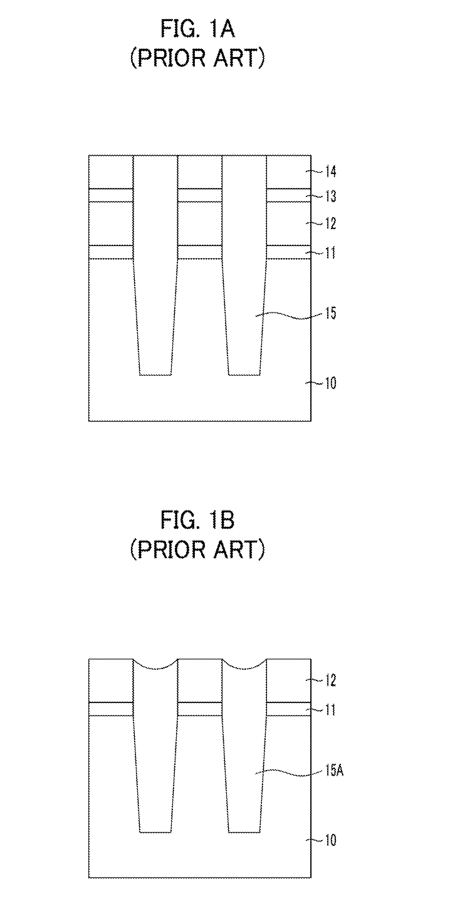
However, when phosphoric acid is used in this process for removing the pad nitride film 14, not only the pad nitride film 14 but also the SOD oxide film 15 are etched due to a decrease in the etching selectivity for the nitride film with respect to the oxide film, which may make it difficult to control the effective field oxide height (EFH).
Thus, a wet-etching time sufficient for removal of the nitride film may not be ensured, or an additional process is required, which results in changes that adversely affect the device characteristics.

Method used


Image

  • Etching composition and method for fabricating semiconductor device using the same
  • Etching composition and method for fabricating semiconductor device using the same
  • Etching composition and method for fabricating semiconductor device using the same

Examples


examples 1 to 12

[0097]A silyl phosphate compound represented by the above formula 1 and phosphoric acid were mixed with each other at the weight ratios shown in Table 1 below in a balance of deionized water, to prepare etching compositions of the present invention. A 85% aqueous solution of phosphoric acid was used for these Examples. Using the etching compositions, etching for a nitride film and an oxide film was carried out at a process temperature of 157° C. Etch rate and selectivity for the nitride film and the oxide film were measured using an ellipsometer (NANO VIEW, SEMG-1000) that is a film thickness measurement system. The results of the measurement are shown in Table 2 below. The etch rate was determined by etching each of the films for 300 seconds and measuring the difference between the thickness of each film before etching and the film thickness of each film after etching. Thus, the etch rate is obtained by dividing the thickness difference by the etching time (minute). The etching sel...


PUM


Abstract

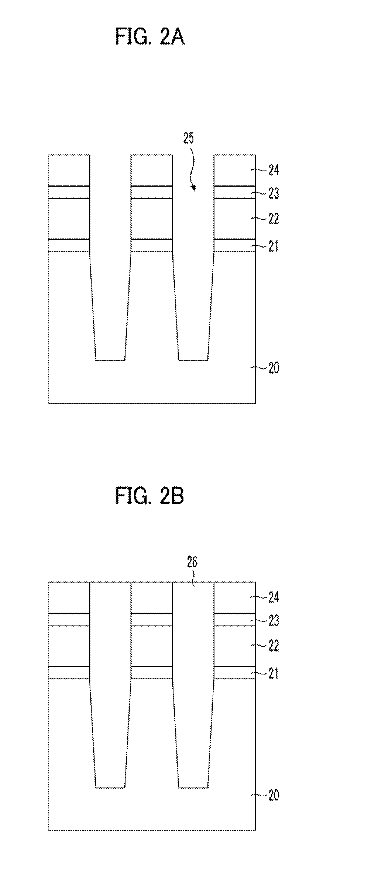
The present invention provides an etching composition, comprising a silyl phosphate compound, phosphoric acid and deionized water, and a method for fabricating a semiconductor, which includes an etching process employing the etching composition. The etching composition of the invention shows a high etching selectivity for a nitride film with respect to an oxide film. Thus, when the etching composition of the present invention is used to remove a nitride film, the effective field oxide height (EEH) may be easily controlled by controlling the etch rate of the oxide film. In addition, the deterioration in electrical characteristics caused by damage to an oxide film or etching of the oxide film may be prevented, and particle generation may be prevented, thereby ensuring the stability and reliability of the etching process.

Description

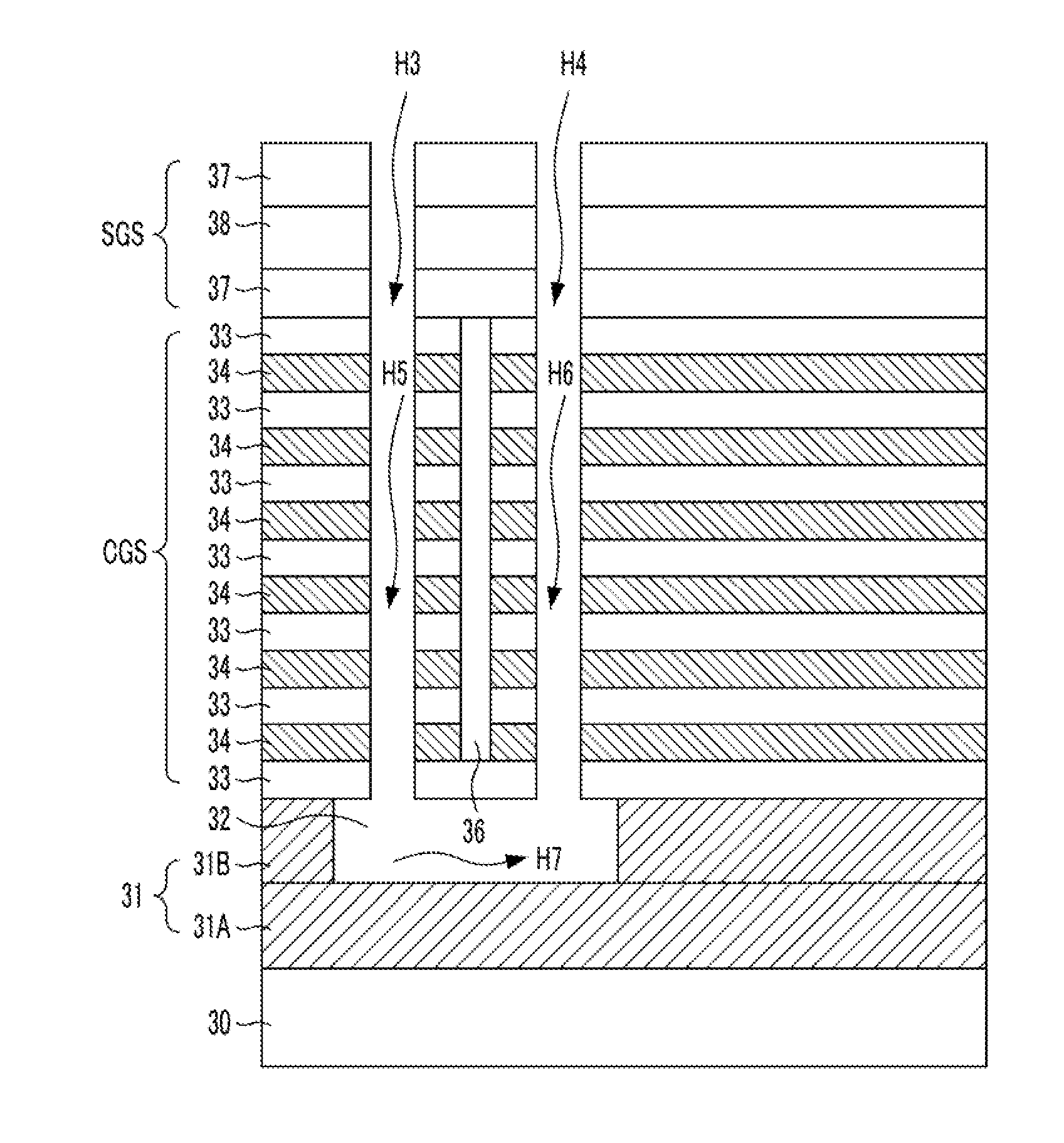
CROSS-REFERENCE TO RELATED APPLICATIONS[0001]The present application claims priority of Korean Patent Application No. 10-2011-0136430, filed on Dec. 16, 2011, which is incorporated herein by reference in its entirety.BACKGROUND[0002]1. Field[0003]Exemplary embodiments of the present invention relate to an etching composition, and more particularly, to a high-selectivity etching composition capable of selectively removing a nitride film while minimizing the etch rate of an oxide film and to a method for fabricating a semiconductor, which includes an etching process employing the etching composition.[0004]2. Description of the Related Art[0005]In semiconductor fabrication processes, oxide films such as a silicon oxide film (SiO2) and nitride films such as a silicon nitride film (SiNx) are typically used as insulating films. These oxide and nitride films may be used alone or stacked alternately with each other. In addition, these oxide and nitride films are used as hard masks for condu...

Claims


Application Information

Patent Timeline
IPC IPC(8): H01L21/306H01L29/66
CPCH01L21/30604H01L29/66666H01L21/31111H01L27/11582H01L29/861H01L27/11556H01L29/66136H10B41/27H10B43/27C09K13/04C09K13/06
Inventor CHO, SUNG-HYUKHONG, KWONPARK, HYUNG-SOONKIM, GYU-HYUNHAN, JI-HYELIM, JUNG-HUNLEE, JIN-UKPARK, JAE-WANJUNG, CHAN-KEUN
Owner SK HYNIX INC
Learn More