

Etching composition, method for etching insulating layer of semiconductor devices and method for preparing semiconductor devices
a technology of etching composition and semiconductor devices, applied in the direction of basic electric elements, electrical equipment, chemistry apparatus and processes, etc., can solve the problems of difficult adjustment of the effective field oxide height (efh), difficulty in handling, and defect in the etching removal process of nitride films, etc., to achieve high selection ratio
- Summary
- Abstract
- Description
- Claims
- Application Information
AI Technical Summary
Benefits of technology
Problems solved by technology
Method used
Image

Examples
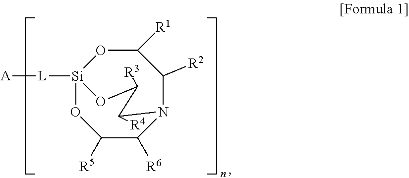
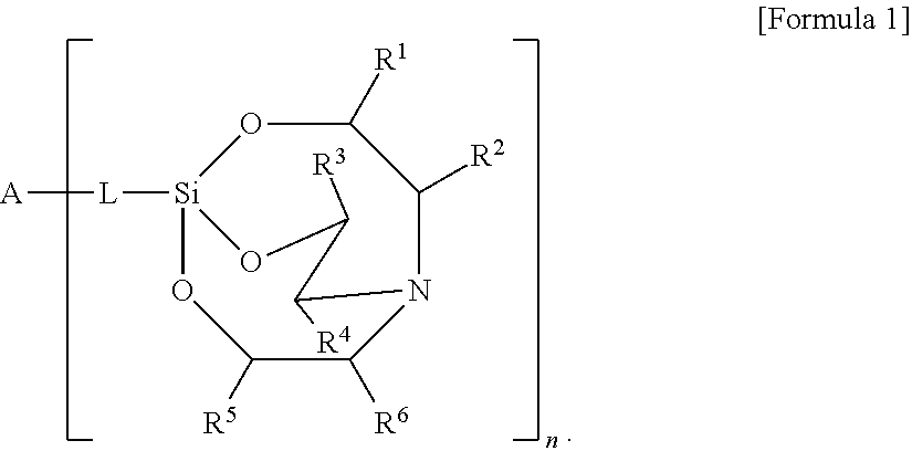
synthesis example 1
[0098]14.9 g of triethanolamine and 20.0 mL of methyl triethoxysilane were added to a 100 mL round bottom flask, heated to 130° C. and stirred for 2 hours.
[0099]After ethanol was then removed under reduced pressure, the mixture was stirred for an additional 2 hours and cooled to room temperature. 14.4 g of a purified silane compound (1-methyl-2,8,9-trioxa-5-aza-1-silabicyclo[3.3.3]undecane; silane compound A) as shown in the following formula through toluene re-slurry (GC / FID purity 99.8%):
[0100]
[0101]1H-NMR (CDCl3) 3.68 (t, J=5.5 Hz, 6H), 2.73 (t, J=5.5 Hz, 6H), −0.21 (s, 3H)
synthesis example 2
[0102]14.9 g of triethanolamine and 23.4 mL of aminopropyl triethoxysilane were added to a 100 mL round bottom flask, heated to 130° C. and stirred for 2 hours.
[0103]After ethanol was then removed under reduced pressure, the mixture was stirred for additional 2 hours and cooled to room temperature. 21.9 g of a purified silane compound (3-(2,8,9-trioxa-5-aza-1-silabicyclo[3.3.3]undecan-1-yl)pro pan-1-amine; silane compound B) as shown in the following formula through distillation under reduced pressure:
[0104]
[0105]1H-NMR (CDCl3) 3.66 (t, J=5.5 Hz, 6H), 2.71 (t, J=5.5 Hz, 6H), 2.52 (t, J=7.0 Hz, 2H), 1.42 (qui, J=9.0 Hz, 2H), 1.19 (br, 2H), 2.00 (t, J=8.5 Hz, 2H)
synthesis example 3
[0106]14.9 g of triethanolamine and 20.0 mL of 1-[3-(trimethoxysilyl)propyl]urea and 20 mL of toluene were added to a 100 mL round bottom flask, heated to 130° C. and stirred for 2 hours.
[0107]After ethanol was then removed under reduced pressure, the mixture was stirred for additional 2 hours and cooled to room temperature.
[0108]The thus-prepared white solid was filtered, washed with toluene and vacuum-dried to synthesize 12.4 g of a silane compound (1-(3-(2,8,9-trioxa-5-aza-1-silabicyclo[3.3.3]undecan-1-yl) propyl)urea; silane compound C) (GC / FID purity 99.5%) as shown in the following formula:
[0109]
[0110]1H-NMR (CDCl3) 3.69 (t, J=5.5 Hz, 6H), 3.39 (t, J=7.0 Hz, 2H), 2.73 (t, J=5.5 Hz, 6H), 1.47 (qui, J=9.0 Hz, 2H), 2.03 (t, J=8.5 Hz, 2H)
PUM
| Property | Measurement | Unit |
|---|---|---|
| temperature | aaaaa | aaaaa |
| temperature | aaaaa | aaaaa |
| temperature | aaaaa | aaaaa |
Abstract
Description
Claims
Application Information