
Composition for etching, method for etching insulator and method for manufacturing semiconductor device, and novel compounds

a technology of etching insulator and semiconductor device, which is applied in the direction of electrical equipment, chemical instruments and processes, organic chemistry, etc., can solve the problems of reducing the selection ratio between the etching selection ratio the oxide film, affecting the etching process, and affecting the etching effect of the nitride film. achieve the effect of high selection ratio

Pending Publication Date: 2021-10-07
SK INNOVATION CO LTD +1
View PDF0 Cites 0 Cited by
  • Summary
  • Abstract
  • Description
  • Claims
  • Application Information

AI Technical Summary

Benefits of technology

[0009]An aspect of the present disclosure is to provide an etching composition having a high selection ratio, which can selectively remove a nitride film while minimizing an etching rate of an oxide film, without causing problems such as particle generation having adverse effects on device characteristics.
[0010]Another aspect of the present disclosure is to provide an etching composition having excellent storage stability.

Problems solved by technology

The deionized water is added for preventing a decrease in an etching rate and a change in etching selectivity of the nitride film to an oxide film; however, there is a problem in that defects arise in a nitride film etching removal process even with a minute change in an amount of supplied deionized water.
In addition, phosphoric acid is a strong acid and corrosive, thereby leading to difficulties in handling.
This technology, however, results in reducing an etching selection ratio of the nitride film and the oxide film.
However, the silicic acid or silicate has a problem of generating particles which may affect a substrate, thereby being inappropriate for a semiconductor manufacturing process.
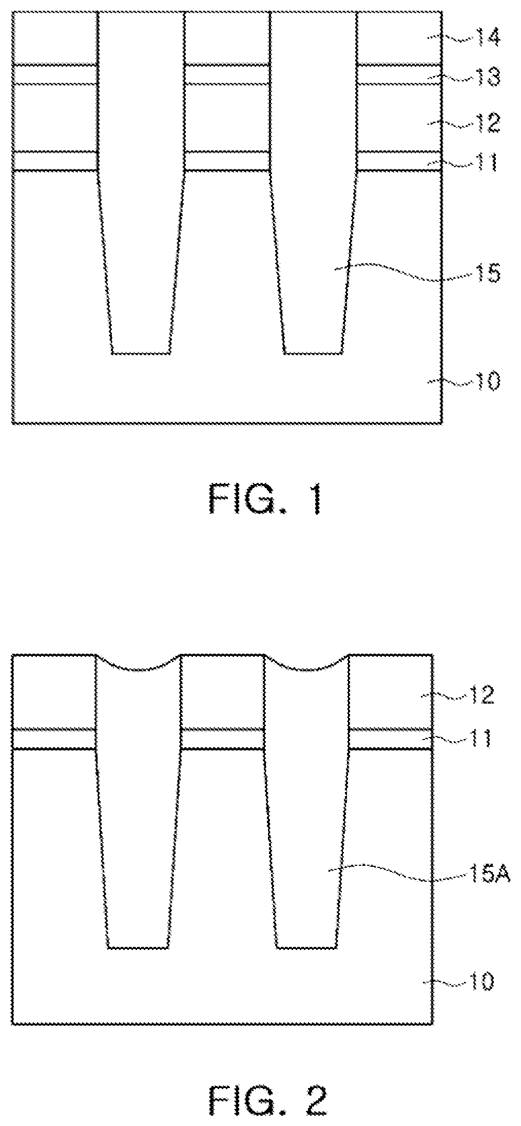
In the meantime, when phosphoric acid is used in a wet etching process for removing the nitride film, not only the nitride film but also an SOD oxide film may be etched due to a reduced etching selection ratio between the nitride film and the oxide film, whereby it is difficult to adjust an effective field oxide height (EFH).
Accordingly, a sufficient wet etching time for removing the nitride film may not be secured, or an additional process may be needed, causing a change in device characteristics and having adverse effects thereon.
Meanwhile, a silane-based additive, which is an additive added to a conventional etching composition, has solubility too low to secure optimal solubility, thereby causing precipitation of particles in the etching solution composition and abnormal growth of a substrate.
Such particles may remain on a silicon substrate, resulting in a defect of a device implemented thereon, or in failure of equipment used in an etching process or a washing process.

Method used


Image

  • Composition for etching, method for etching insulator and method for manufacturing semiconductor device, and novel compounds
  • Composition for etching, method for etching insulator and method for manufacturing semiconductor device, and novel compounds
  • Composition for etching, method for etching insulator and method for manufacturing semiconductor device, and novel compounds

Examples


synthesis example 1

[0098]7.0 g of methyl(3-triethoxysilyl)propyl carbonate, 3.7 g of triethanolamine, 35 mL of tetrahydrofuran and 0.2 g of sodium hydroxide were added to a 100 mL round bottom flask, heated to 50° C. and stirred for 4 hours.

[0099]Tetrahydrofuran was removed under reduced pressure to obtain a white solid.

[0100]Thus-obtained white solid was subject to ethyl acetate re-slurry to synthesis 5.1 g of purified 3-(2,8,9-trioxa-5-aza-1-silabicyclo[3.3.3]undecan-1-yl)propyl methylcarbonate (additive 2):

[0101]1H-NMR (CDCl3) 4.21 (t, 2H), 3.89 (t, 6H), 3.79 (s, 3H), 2.55 (t, 6H), 1.60 (m, 2H), 0.58 (t, 2H)

synthesis example 2

[0102]7.8 g of N-(3-(triethoxysilyl)propyl)-1H-imidazole-1-carboxamide, 3.7 g of triethanolamine, 35 mL of tetrahydrofuran and 0.2 g of sodium hydroxide were added to a 100 mL round bottom flask, heated to 50° C. and stirred for 4 hours.

[0103]Tetrahydrofuran was removed under reduced pressure to obtain a yellow solid.

[0104]Thus-obtained yellow solid was subject to ethyl acetate re-slurry to synthesis 5.5 g of purified N-(3-(2,8,9-trioxa-5-aza-1-silabicyclo[3.3.3]undecan-1-yl)propyl)-1H-imidazole-1-carboxamide (additive 3):

[0105]1H-NMR (CDCl3) 8.14 (s, 1H), 7.46 (d, 1H), 7.14 (d, 1H), 3.89 (t, 6H), 3.18 (t, 2H), 2.55 (t, 6H), 1.60 (m, 2H), 0.58 (t, 2H)

synthesis example 3

[0106]7.7 g of methyl(3-(triethoxysilyl)propyl)carbamodithioate, 3.7 g of triethanolamine, 35 mL of tetrahydrofuran and 0.2 g of sodium hydroxide were added to a 100 mL round bottom flask, heated to 50° C. and stirred for 4 hours.

[0107]Tetrahydrofuran was removed under reduced pressure to obtain a yellow solid.

[0108]Thus-obtained yellow solid was subject to ethyl acetate re-slurry to synthesis 5.8 g of purified methyl(3-(2,8,9-trioxa-5-aza-1-silabicyclo[3.3.3]undecan-1-yl)propyl)carbamodithioate (additive 4):

[0109]1H-NMR (CDCl3) 3.89 (t, 6H), 2.87 (t, 2H), 2.55 (m, 9H), 1.60 (m, 2H), 0.58 (t, 2H)


PUM

PropertyMeasurementUnit
temperatureaaaaaaaaaa

Abstract

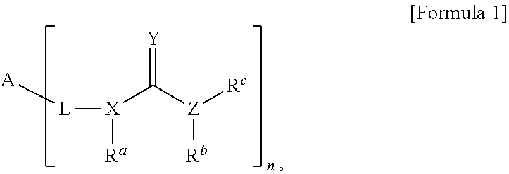
An etching composition contains phosphoric acid, phosphoric anhydride, a compound represented by the following Formula 1, and a silane compound comprising at least one silicon (Si) atom, excluding the compound represented by Formula 1:wherein, in Formula 1, A is an n-valent radical, where n is an integer of 1 to 6, L is a direct bond or hydrocarbylene, Y is selected from NR1, O, PR2 and S, where R1 to R2 are independently hydrogen, halogen, a substituted unsubstituted hydrocarbyl group, or non-hydrocarbyl group, X and Z are independently selected from N, O, P and S, and Ra to Rc are independently an unshared electron pair, hydrogen, or a substituted or unsubstituted hydrocarbyl group.

Description

CROSS-REFERENCE TO RELATED APPLICATION(S)[0001]This application is a divisional of U.S. application Ser. No. 16 / 886,944, filed on May 29, 2020, which claims benefit of priority to Korean Patent Application No. 10-2019-0063737 filed on May 30, 2019 in the Korean Intellectual Property Office, the disclosure of which is incorporated herein by reference m its entirety.BACKGROUND1. Field[0002]The present disclosure relates to an etching composition, particularly, to an etching composition having a high selection ratio and capable of selectively removing a nitride film while minimizing an etching rate of an oxide film, a method of etching an insulator film, and a method of manufacturing a semiconductor device to which the etching method is applied. Furthermore, the present disclosure relates a silane compound appropriate for being used as an additive of the etching composition.2. Description of Related Art[0003]An oxide film, such as a silicon oxide (SiO2) film, and a nitride film, such a...

Claims


Application Information

Patent Timeline
Patent Type & Authority Applications(United States)
IPC IPC(8): C09K13/06C07F7/18H01L21/4757
CPCC09K13/06H01L21/47573C07F7/1804H01L21/31111
Inventor KIM, CHEOL WOOSEON, MIN KYUNGSHIM, YU NAKWAK, JAE HOONKIM, YOUNG BOMLEE, JONG HOJO, JIN KYUNG
Owner SK INNOVATION CO LTD
Learn More