Semiconductor light-emitting device, method for producing same, and display device

Active Publication Date: 2013-06-27
ROHM CO LTD
View PDF3 Cites 10 Cited by
  • Summary
  • Abstract
  • Description
  • Claims
  • Application Information

AI Technical Summary

Benefits of technology

[0009]The present invention has been proposed under the foregoing situation. It is therefore an object of the present invention to provide a semiconductor light-emitting device that can be manufactured in a smaller size,

Problems solved by technology

This is another obstacle that impedes the reduction in size of the semiconductor light-emitting device 901.
However, this process requires considerable time and labor, and hence constitutes a bot

Method used


Image

  • Semiconductor light-emitting device, method for producing same, and display device
  • Semiconductor light-emitting device, method for producing same, and display device
  • Semiconductor light-emitting device, method for producing same, and display device

Examples


Embodiment Construction

[0057]Preferred embodiments of the present invention will be described below with reference to the accompanying drawings.

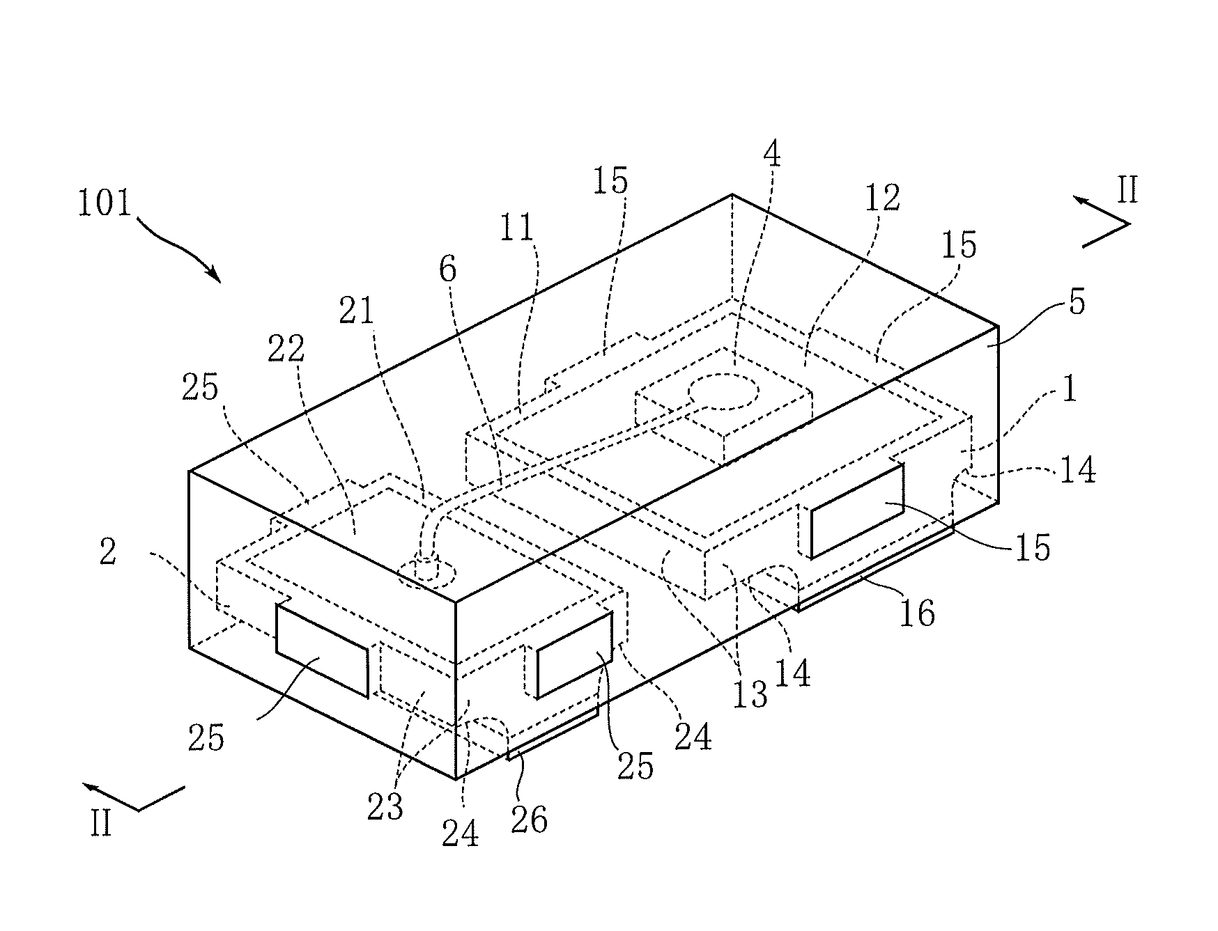
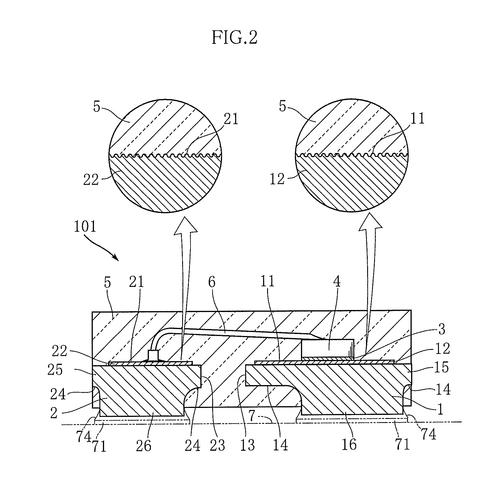
[0058]FIGS. 1 to 3 depict an example of a semiconductor light-emitting device according to an embodiment of the present invention. The semiconductor light-emitting device 101 according to this embodiment includes a pair of leads 1, 2, a metal joint layer 3, an LED chip 4, and a resin package 5. In FIG. 1, the metal joint layer 3 is not shown for the sake of convenience. The semiconductor light-emitting device 101 is configured as a small and thin device, having dimensions of approximately 0.6 mm in length, 0.3 mm in width, and 0.2 mm in thickness.

[0059]The pair of leads 1, 2 serve to support the LED chip 4 and supply power thereto. The leads 1, 2 are formed of Cu or an alloy thereof, in a thickness of slightly less than 0.1 mm. The lead 1 includes a main surface 11, four side faces 13, two buried surfaces 14, three drawn-out portions 15, and a mounting terminal 16...


PUM


Abstract

A semiconductor light-emitting device (101) includes an LED chip (4), a lead (1) having a main surface (11) on which the LED chip (4) is mounted, and a resin package (5) covering the LED chip (4). The main surface (11) is roughened, and the main surface (11) is held in contact with the resin package (5). These configurations contribute to the downsizing of the semiconductor light-emitting device (101).

Description

TECHNICAL FIELD[0001]The present invention relates to a semiconductor light-emitting device including semiconductor light-emitting elements, while also relating to a manufacturing Method thereof and a display device such as a 7-segment display and a dot matrix display.BACKGROUND ART[0002]FIG. 17 depicts a conventional semiconductor light-emitting device (see e.g. Patent document 1). The semiconductor light-emitting device 901 shown in FIG. 17 includes an LED chip 912 bonded on a substrate 910. The LED chip 912 and a wire 913 are encapsulated in a resin package 914.[0003]In recent years, there has been a growing demand for reduction in size, for example with respect to mobile phones. Accordingly, the semiconductor light-emitting device 901 is required to be made smaller. On the other hand, the resin package 914 has to have a size that can properly cover the LED chip 912 and the wire 913. The substrate 910 includes orifices 911 formed on the respective end portions thereof, for electr...

Claims


Application Information

Patent Timeline
IPC IPC(8): H01L33/08H01L33/52H01L33/50
CPCH01L24/48H01L33/486H01L2224/97H01L2224/73265H01L2224/32245H01L24/97H01L33/52H01L33/50H01L33/08H01L2924/01322H01L2924/01033H01L2924/014H01L2924/01088H01L2924/01082H01L2924/01079H01L33/60H01L33/62H01L2224/48091H01L2224/48247H01L2224/48471H01L2924/01004H01L2924/01029H01L2924/01032H01L2924/01047H01L2924/0105H01L2924/00014H01L2924/00H01L2924/00012H01L24/73H01L2924/181H01L2224/45099H01L2224/05599H01L25/0753H01L33/22H01L33/507H01L33/54H01L33/56H01L2933/005H01L2933/0066
Inventor MINESHITA, KENTARO
Owner ROHM CO LTD
Why Eureka
Try Eureka