ESD protection circuit

a protection circuit and integrated circuit technology, applied in emergency protection arrangements for limiting excess voltage/current, electrical equipment, semiconductor devices, etc., can solve problems such as undesirable signal loss, related cmos ic products becoming more susceptible to damag

Active Publication Date: 2013-06-27
TAIWAN SEMICON MFG CO LTD
View PDF5 Cites 9 Cited by
  • Summary
  • Abstract
  • Description
  • Claims
  • Application Information

AI Technical Summary

Problems solved by technology

All of these processes cause the related CMOS IC products to become more susceptible to damage due to ESD events.
However, conventional ESD protection circuits cause undesirable signal losses.

Method used


Image

  • ESD protection circuit
  • ESD protection circuit
  • ESD protection circuit

Examples


Embodiment Construction

[0010]This description of the exemplary embodiments is intended to be read in connection with the accompanying drawings, which are to be considered part of the entire written description.

[0011]The improved electrostatic discharge (“ESD”) circuits disclosed herein advantageously protect high-speed circuits (e.g., circuits having data rates of 10 Gb / s and beyond and operating frequencies of greater than one gigahertz) with reduced signal loss.

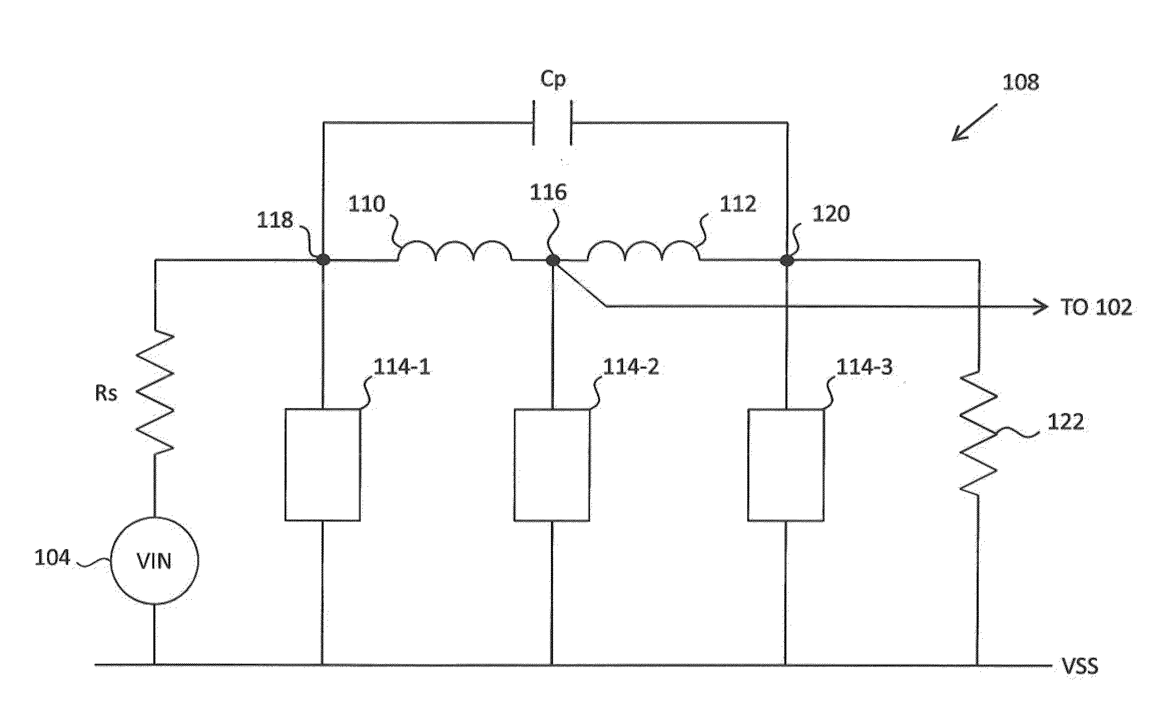
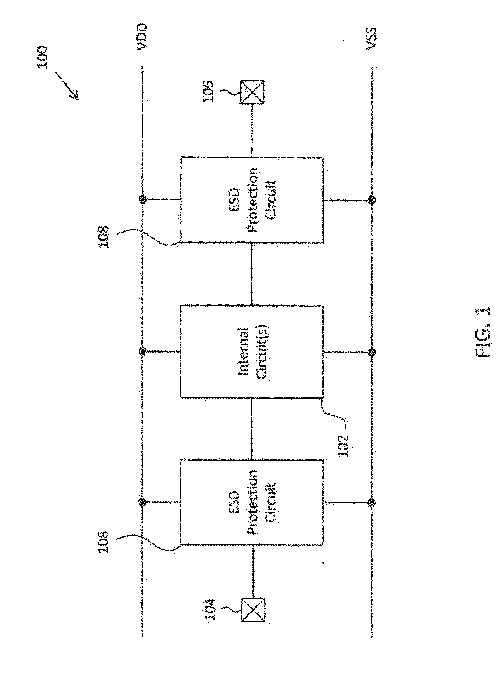
[0012]FIG. 1 illustrates an integrated circuit 100 including an internal circuitry 102 disposed between an input pad 104, and an output pad 106. ESD protection circuitry 108 is disposed between the internal circuit(s) 102 and the input pad 104 as well as between the internal circuit(s) 102 and the output pad 106.

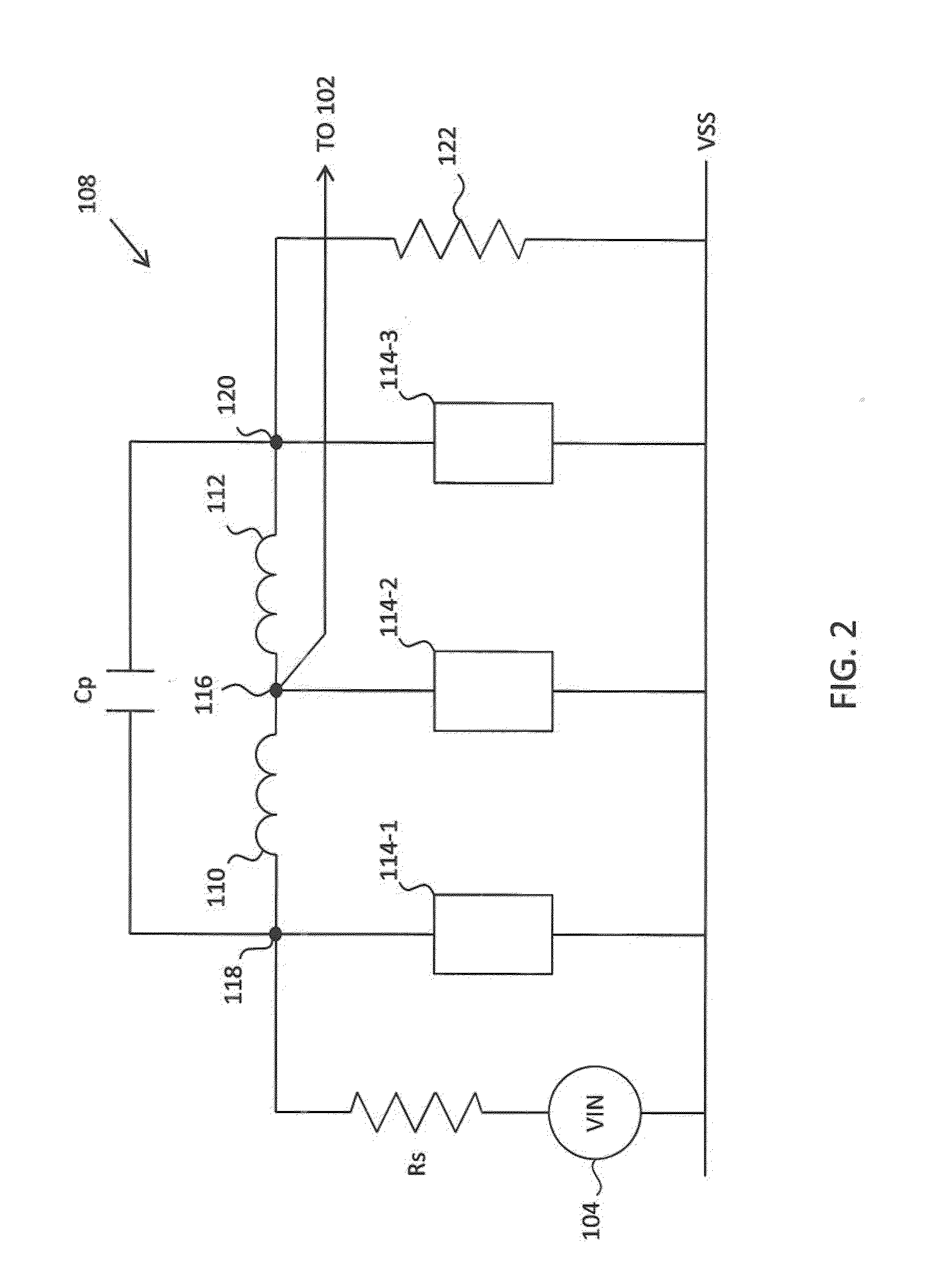
[0013]FIG. 2 illustrates one example of the equivalent circuit of an improved ESD protection circuit 108. As shown in FIG. 2, ESD protection circuit 108 includes a pair of inductors 110, 112 and a plurality of distributed protection devic...


PUM


Abstract

An electrostatic discharge protection circuit includes an input node coupled to receive an input signal and an output node coupled to output the input signal to an internal circuit. A first inductor is coupled to the input node and to the output node, and a second inductor is coupled to the output node and to a first power supply node through a resistance. A plurality of protection devices are coupled to the first and second inductors and are disposed in parallel with each other.

Description

FIELD OF DISCLOSURE[0001]The disclosed systems and methods relate to integrated circuits. More specifically, the disclosed systems and methods relate to integrated circuits with improved electrostatic discharge (ESD) protection circuits.BACKGROUND[0002]With the continued miniaturization of integrated circuit (IC) devices, the current trend is to produce integrated circuits having shallower junction depths, thinner gate oxides, lightly-doped drain (LDD) structures, shallow trench isolation (STI) structures, and self-aligned silicide (salicide) processes, all of which are used in advanced sub-quarter-micron complementary metal oxide semiconductor (CMOS) technologies. All of these processes cause the related CMOS IC products to become more susceptible to damage due to ESD events. Therefore, ESD protection circuits are built onto the chip to protect the devices and circuits on the IC from ESD damage. ESD protection circuits are typically provided for input / output (“I / O”) pads. However, ...

Claims


Application Information

Patent Timeline
Patent Type & Authority Applications(United States)
IPC IPC(8): H02H9/04
CPCH02H9/046H01L27/0288
Inventor CHU, LI-WEILIN, CHUN-YUTSAI, SHIANG-YUKER, MING-DOUTSAI, MING-HSIENHSU, TSUN-LAIJOU, CHEW-PU
Owner TAIWAN SEMICON MFG CO LTD
Why Eureka
Try Eureka