
Address fault detection circuit

a fault detection and address technology, applied in the field of word line faults in memories, can solve the problems of large chip area, memory failures can have a bigger impact, and the failure of integrated circuit memories to fail,

Active Publication Date: 2016-02-16
NXP USA INC
View PDF7 Cites 3 Cited by
  • Summary
  • Abstract
  • Description
  • Claims
  • Application Information

AI Technical Summary

Benefits of technology

Enables high-speed and area-efficient detection of transient address faults, allowing for timely correction of word line faults without the need for large ROM arrays, thereby improving memory system reliability and reducing chip area usage.

Problems solved by technology

Integrated circuit memories may fail in a variety of ways, and memory failures can have bigger impact as memories are increasingly used in various computer systems and applications.
In the class of memory failures relating to operation of the word lines, one type of fault (called a “no word line select” fault) occurs when no word line is enabled when the memory is intended to be accessed.
Another type of fault (called a “multiple word line select” fault) occurs when more than one word line is enabled in the same array.
Yet another type of fault (called a “false word line select” fault) occurs when a word line in an array is incorrectly asserted while another word line is incorrectly deasserted.
For example, transient address faults can be caused by a particle strike in an address decoder, while non-transient address faults can be caused by a physical defect in the memory hardware.
However, address ROM banks require significant chip area, especially when using a multi-bank array architecture with multiple different word lines since every bank needs a ROM bank.

Method used


Image

  • Address fault detection circuit
  • Address fault detection circuit
  • Address fault detection circuit

Examples


Embodiment Construction

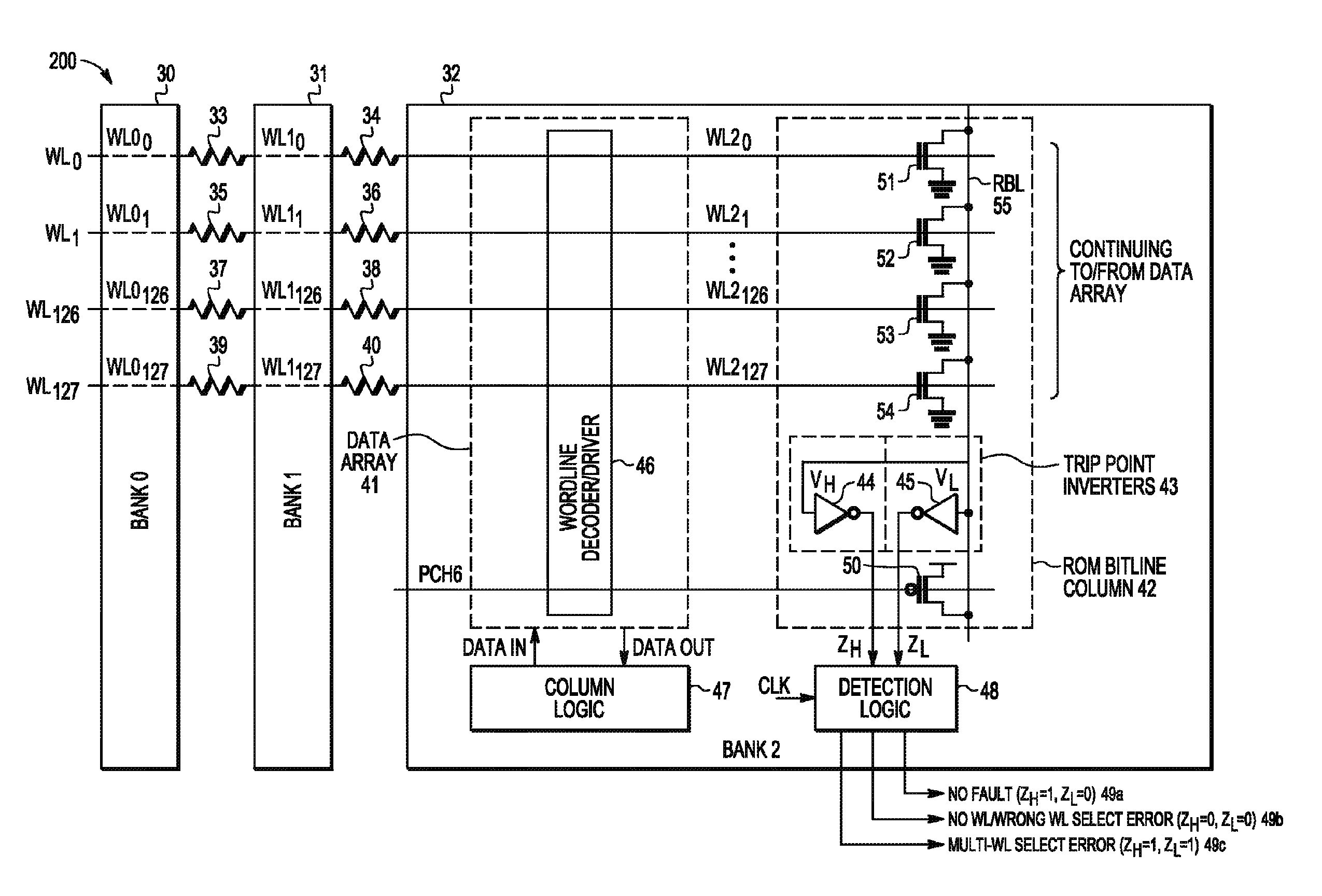
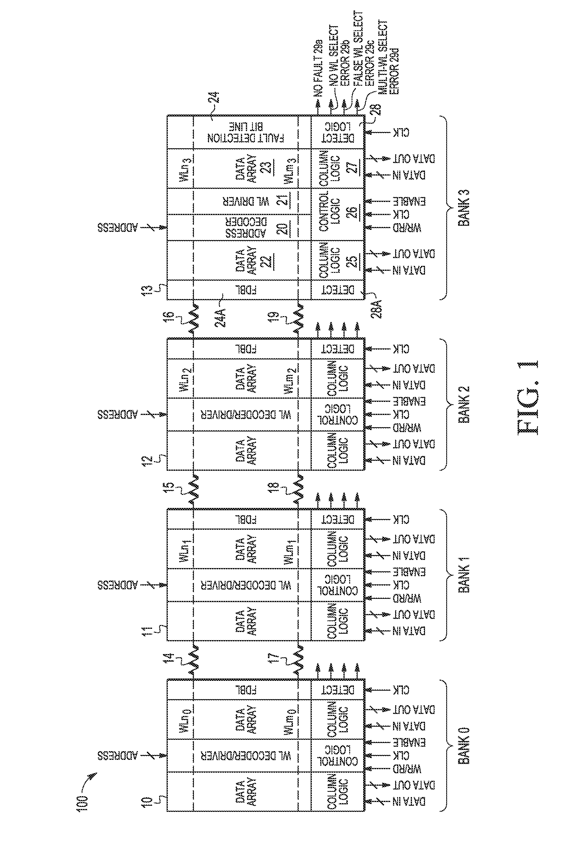
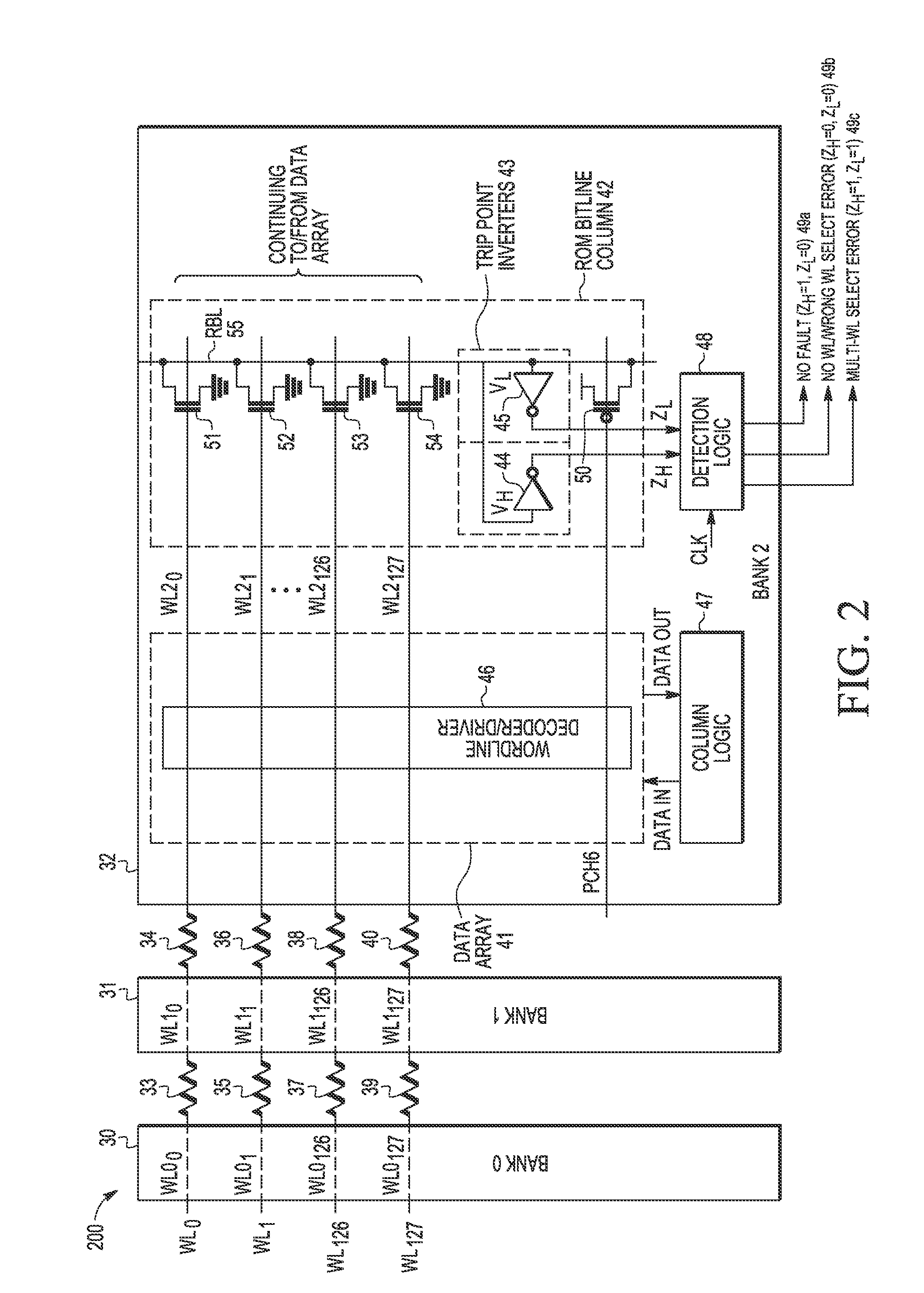
[0014]A method and apparatus are described for quickly and efficiently detecting transient address faults in the address decoders of a multi-bank memory system that would cause “no word line select,”“false word line select,” and “multiple word line select” failure modes. In selected embodiments, high-speed address fault detection is provided by coupling word lines split across multiple banks with resistive elements or switched word line connection circuits so that the interaction or contention between split word lines during an address fault causes a unique voltage level at a fault detection bit line at each bank, depending on the fault type. In an example embodiment where corresponding word lines in adjacent banks are connected across a resistor or weak pass transistor(s), a word line address fault at one of the banks will cause the word line driver at that bank to go into contention, but due to the resistive coupling with corresponding word lines in other banks, the resistively co...


PUM


Abstract

A semiconductor memory device and method of operation are provided for a multi-bank memory array (100) with an address fault detector circuit (24, 28) connected to split word lines (WLn-WLm) across multiple banks, where the address fault detector circuit includes at least a first MOSFET transistor (51-54) connected to each word line for detecting an error-free operation mode and a plurality of different transient address faults including a “no word line select,”“false word line select,” and “multiple word line select” failure mode at one of the first and second memory banks. In selected embodiments, the address fault detector provides resistive coupling (33-40) between split word lines across multiple banks to create interaction or contention between split word lines to create a unique voltage level on a fault detection bit line during an address fault depending on the fault type.

Description

BACKGROUND OF THE INVENTION[0001]1. Field of the Invention[0002]The present invention is directed in general to word line faults in memories. In one aspect, the present invention relates to address fault detection for integrated circuit memories and associated methods of operation.[0003]2. Description of the Related Art[0004]Integrated circuit memories may fail in a variety of ways, and memory failures can have bigger impact as memories are increasingly used in various computer systems and applications. There are a variety of different ways for a memory to fail, including address decoder faults, word line faults, pre-decoder faults, address latch faults. In the class of memory failures relating to operation of the word lines, one type of fault (called a “no word line select” fault) occurs when no word line is enabled when the memory is intended to be accessed. Detection for this type of failure is commonly indicated by a signal called “word line on indicator” which indicates whether...

Claims


Application Information

Patent Timeline
Patent Type & Authority Patents(United States)
IPC IPC(8): G11C7/00G11C11/418G11C11/408G11C29/00G11C29/02
CPCG11C29/02G11C11/408G11C11/418G11C29/785G11C11/4087G11C29/808G11C8/08G11C11/41G11C29/024G11C2029/1202
Inventor HOEFLER, ALEXANDER B.REMINGTON, SCOTT I.ZHANG, SHAYAN
Owner NXP USA INC
Learn More