Semiconductor device

a technology of semiconductors and semiconductors, applied in semiconductor devices, electrical equipment, transistors, etc., can solve the problems of short-channel effect, electric characteristics deterioration, transistor deterioration, etc., to achieve high-speed operation, shorten the channel length, and reduce the on-state resistance

Inactive Publication Date: 2013-07-18
SEMICON ENERGY LAB CO LTD
View PDF10 Cites 51 Cited by
  • Summary
  • Abstract
  • Description
  • Claims
  • Application Information

AI Technical Summary

Benefits of technology

The patent text describes a new type of transistor that has a short channel length, which means it has low resistance when in use. This allows it to operate at high speeds. The transistor is designed so that it doesn't have a short-channel effect, which means it's not affected by other components in the semiconductor device it's used in. This makes it possible to create a high-performance semiconductor device that's fast, highly integrated, and low in power consumption. It can also be made more reliable and cost-effective.

Problems solved by technology

The technical problem addressed in this patent text is the deterioration of electric characteristics and the short-channel effect in MOSFETs caused by reduction in the size of the MOSFET and the thickness of the gate insulating film. The text describes various techniques to prevent these effects, such as the use of a high-k material as the material of the gate insulating film, the formation of a special impurity region in the channel formation region, and the formation of an LDD region between the channel formation region and the source or drain region. These techniques aim to improve the operation speed, integration degree, and prevent the short-channel effect while also addressing the issue of hot carriers.

Method used


Image

  • Semiconductor device
  • Semiconductor device
  • Semiconductor device

Examples


embodiment 1

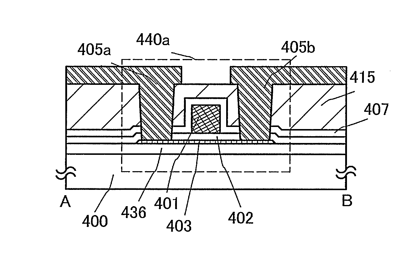
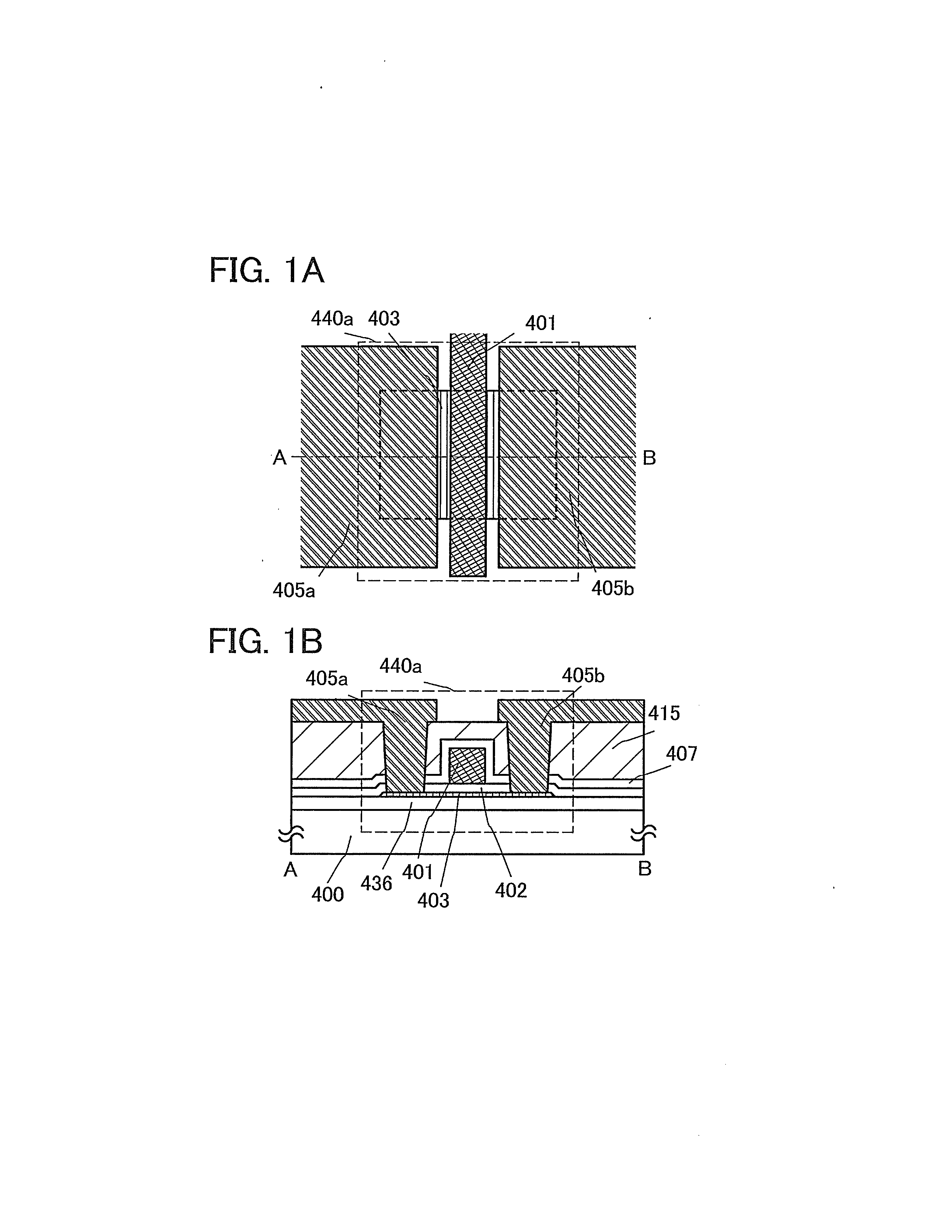
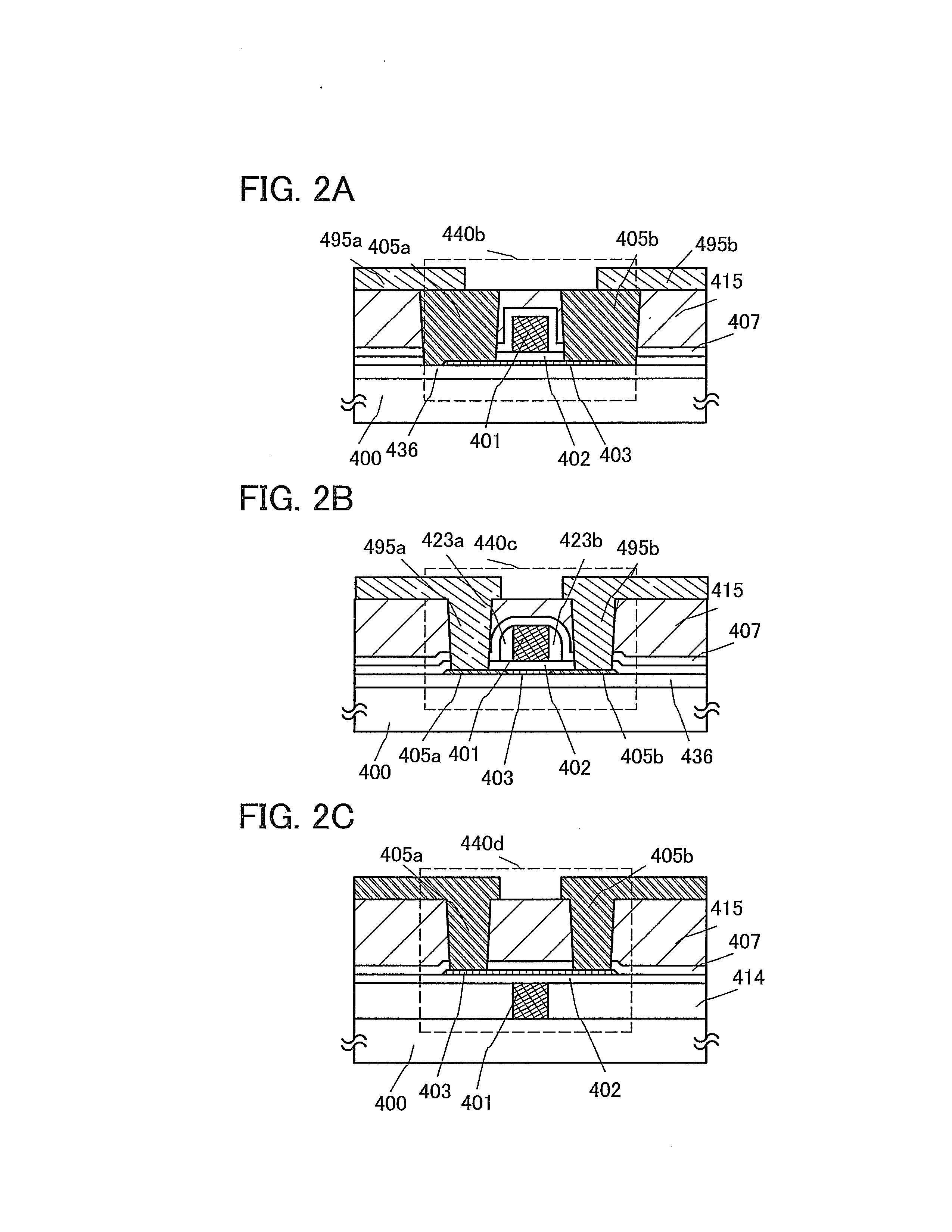
[0098]In this embodiment, embodiments of a semiconductor device and one embodiment of a method for manufacturing the semiconductor device will be described using FIGS. 1A and 1B, FIGS. 2A to 2C, and FIGS. 3A to 3C. In this embodiment, a transistor including an oxide semiconductor film will be described as an example of the semiconductor device.

[0099]The transistor may have a top-gate structure or a bottom-gate structure, and may have a single-gate structure in which one channel formation region is formed, a double-gate structure in which two channel formation regions are formed, or a triple-gate structure in which three channel formation regions are formed. Alternatively, the transistor may have a dual-gate structure including two gate electrode layers positioned above and below a channel formation region with gate insulating films provided therebetween.

[0100]A transistor 440a illustrated in FIGS. 1A and 1B is an example of a top-gate transistor. FIG. 1A is a plan view of the transi...

embodiment 2

[0239]In this embodiment, an embodiment of a semiconductor device and a manufacturing method thereof will be described with reference to FIGS. 17A and 17B, FIGS. 18A to 18C, FIGS. 19A to 19C, and FIGS. 20A to 20C. In this embodiment, a transistor including an oxide semiconductor film will be described as an example of the semiconductor device.

[0240]The transistor may have a top-gate structure or a bottom-gate structure, and may have a single-gate structure in which one channel formation region is formed, a double-gate structure in which two channel formation regions are formed, or a triple-gate structure in which three channel formation regions are formed. Alternatively, the transistor may have a dual-gate structure including two gate electrode layers positioned above and below a channel formation region with gate insulating films provided therebetween.

[0241]FIGS. 17A and 17B illustrate a structure example of a transistor 420. The transistor 420 illustrated in FIGS. 17A and 17B is a...

embodiment 3

[0321]In this embodiment, an example of a semiconductor device which includes the transistor described in this specification, which can hold stored data even when not powered, and which does not have a limitation on the number of write cycles, will be described with reference to drawings.

[0322]FIGS. 5A to 5C illustrate an example of the structure of a semiconductor device. FIGS. 5A to 5C illustrate a cross-sectional view, a plan view, and a circuit diagram, respectively, of the semiconductor device. Here, FIG. 5A corresponds to cross sections taken along line C1-C2 and line D1-D2 in FIG. 5B.

[0323]The semiconductor device illustrated in FIGS. 5A and 5B includes a transistor 160 including a first semiconductor material in a lower portion, and a transistor 162 including a second semiconductor material in an upper portion. The transistor according to one embodiment of the present invention, which is described in Embodiment 1 or 2, can be applied to the transistor 162. This embodiment sh...


PUM


Abstract

The semiconductor device includes a transistor including an oxide semiconductor film having a channel formation region, a gate insulating film, and a gate electrode layer. In the transistor, the channel length is small (5 nm or more and less than 60 nm, preferably 10 nm or more and 40 nm or less), and the thickness of the gate insulating film is large (equivalent oxide thickness which is obtained by converting into a thickness of silicon oxide containing nitrogen is 5 nm or more and 50 nm or less, preferably 10 nm or more and 40 nm or less). Alternatively, the channel length is small (5 nm or more and less than 60 nm, preferably 10 nm or more and 40 nm or less), and the resistivity of the source region and the drain region is 1.9×10⁻⁵ Ω·m or more and 4.8×10⁻³ Ω·m or less.

Description


Claims


Application Information

Patent Timeline
Owner SEMICON ENERGY LAB CO LTD
Why Eureka
Try Eureka