Sonos structure and manufacturing method thereof

Inactive Publication Date: 2013-07-18
SHANGHAI HUALI MICROELECTRONICS CORP
View PDF2 Cites 3 Cited by
  • Summary
  • Abstract
  • Description
  • Claims
  • Application Information

AI Technical Summary

Benefits of technology

The present invention provides improvements for the programming and erasing speed of SONOS devices. A Si-rich nitride layer and a graded silicon nitride layer are used to enhance the structure of the silicon nitride layer in the SONOS. By using a Si-rich silicon nitride layer with shallower trapping levels, the charge-trapping efficiency increases and the programming and erasing speed enhances. The substrate-injected charges can be transferred from the shallow trapping levels to the deep trapping levels of the graded silicon nitride layer through lateral hopping, which makes the device more reliable and increases charge retention time. The SONOS structure not only improves the initial programming and erasing speed of the graded silicon nitride layer, but also can realize various programming and erasing speeds by adjusting the thickness ratio of the Si-rich silicon nitride layer and the graded silicon nitride layer, which provides a wide application scope.

Problems solved by technology

With the miniaturization and microminiaturization of the semiconductor storage devices, it is difficult for the conventional floating-gate storage structure to adapt to the future development due to the excessive laminated thickness of the gate and the high requirements of the insulating property of the tunneling oxide layer.
And based on an extrapolation method, the tapered bandgap structure still exhibits a window of 1.3V after ten years due to the large threshold voltage shift, even though the charge retention ability of the device at room temperature has not be improved.
However, the tapered bandgap structure has less shallow trapping level, which results in the slow initial programming and erasing speed.
Therefore the trapped charges are not easy to escape from the silicon nitride layer and data retention is improved.
However, the structure still cannot provide improvements in the initial programming and erasing speed.

Method used


Image

  • Sonos structure and manufacturing method thereof
  • Sonos structure and manufacturing method thereof
  • Sonos structure and manufacturing method thereof

Examples


Embodiment Construction

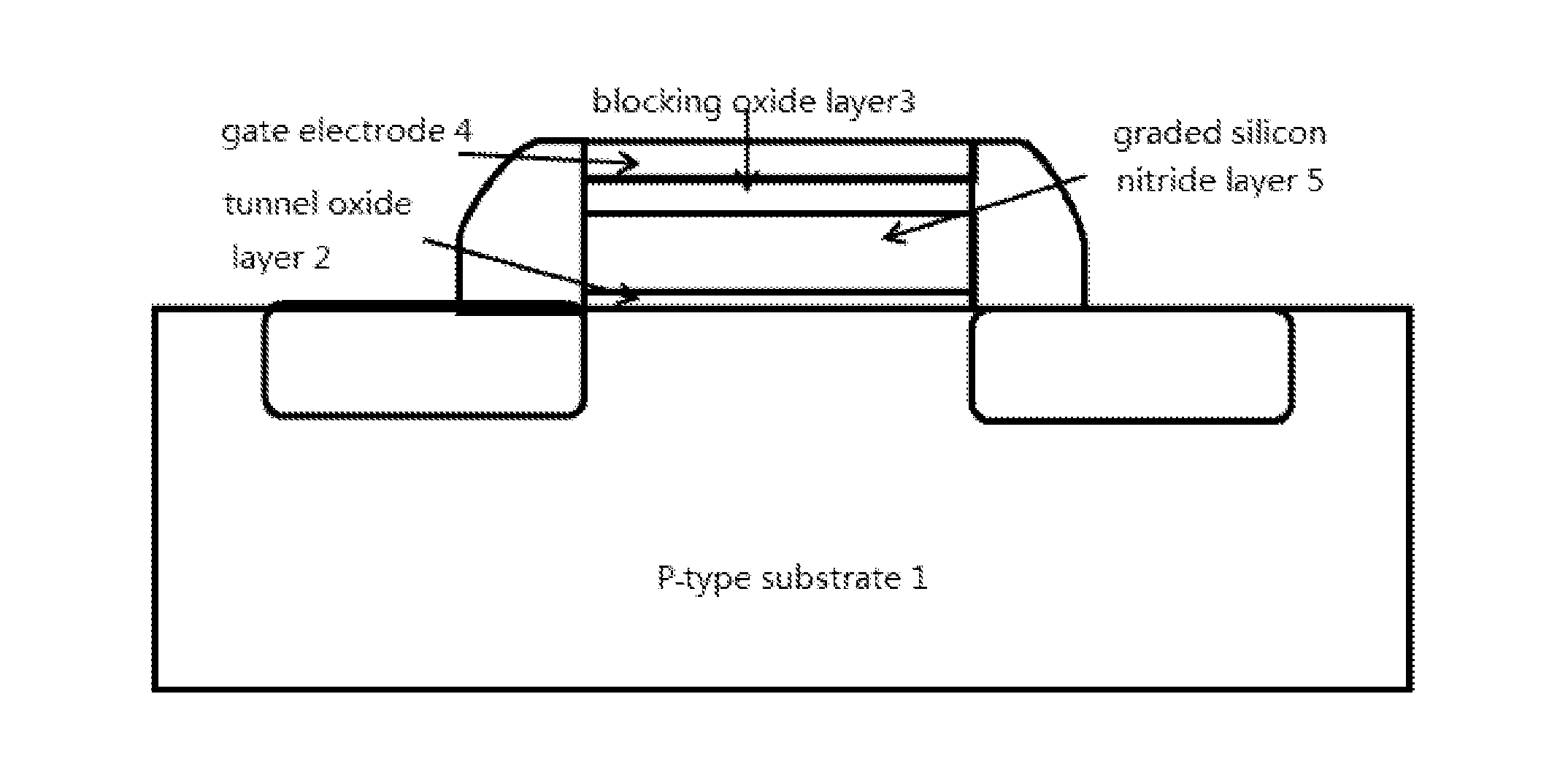
[0021]The SONOS structure and manufacturing method of the SONOS structure of the present invention will be described in further details hereinafter with respect to the embodiments and the accompanying figures, wherein like reference numerals are used throughout the figures to designate similar or equivalent element, the figures are not drawn to scale and they are provided merely to illustrate the invention instead of limiting the scope of the present invention.

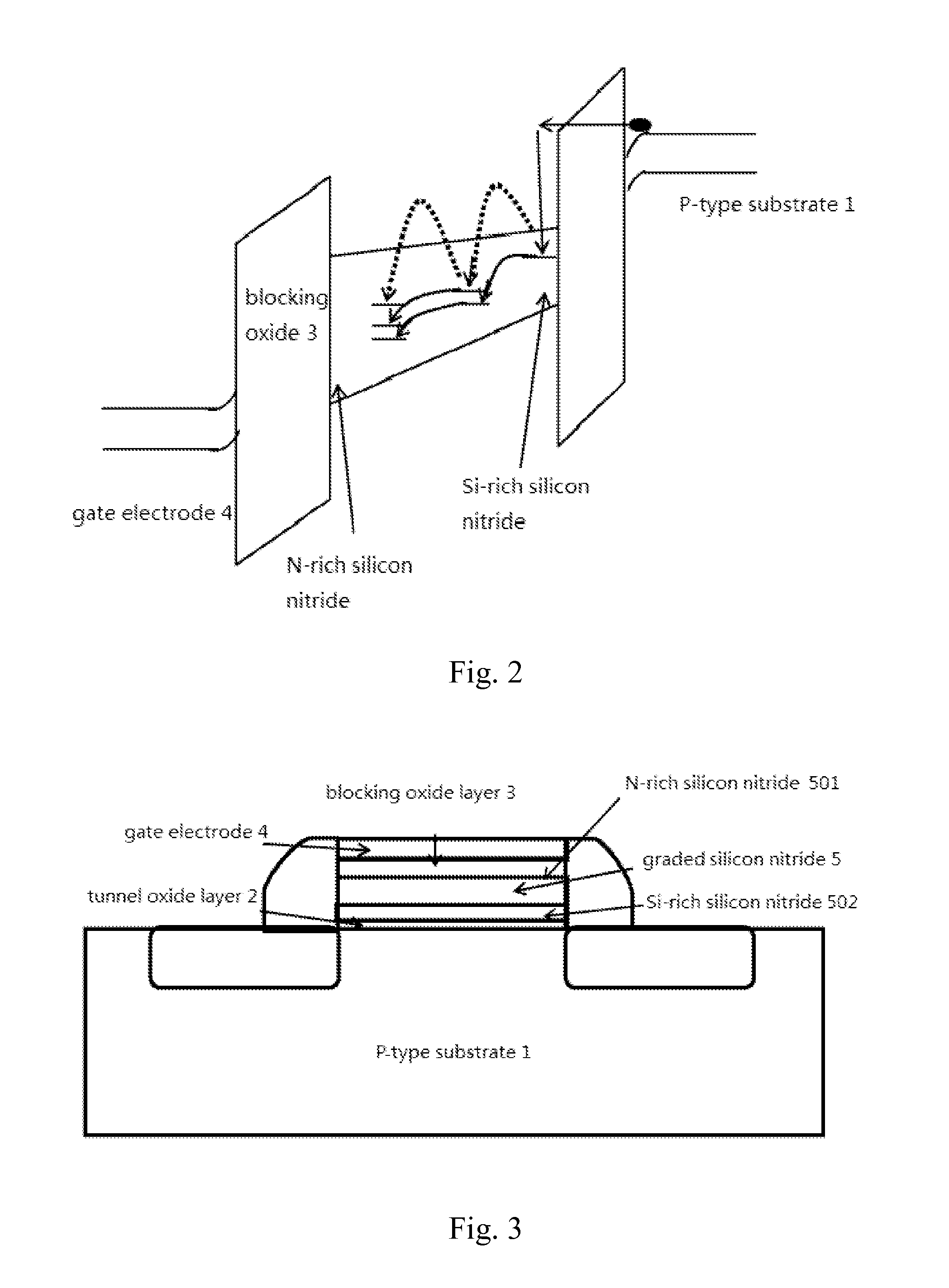
[0022]FIG. 3 is a cross-sectional view showing the SONOS structure having a Si-rich silicon nitride layer and a graded silicon nitride layer in one embodiment of the present invention.

[0023]Referring to FIG. 3, during the manufacturing process of the SONOS structure, a tunneling oxide layer 2 is formed on the P-type substrate 1 at first; then a Si-rich silicon nitride layer 502 is deposited above the tunneling oxide layer 2 and a graded silicon nitride layer 5 with graded silicon content is deposited above the Si-rich silicon ...


PUM


Abstract

The invention provides an SONOS structure and a manufacturing method thereof The manufacturing method comprises: forming a tunneling oxide layer on a substrate; depositing a Si-rich silicon nitride layer above the tunneling oxide layer, wherein the Si / N content ratio of the Si-rich silicon nitride layer is constant; depositing a graded silicon nitride layer having graded silicon content above the Si-rich silicon nitride layer; and depositing a blocking oxide layer; wherein the silicon content of the graded silicon nitride layer is reduced in the direction from the Si-rich silicon nitride layer to the blocking oxide layer. According to the present invention, the Si-rich silicon nitride layer provides shallower trapping levels, which is beneficial to trap the charges and improve the programming and erasing speed. Furthermore, the charge retention time increases due to the constrained charges in the deep trapping levels, thus the reliability of the device enhances.

Description

CROSS-REFERENCE TO RELATED APPLICATION[0001]This application claims the priority benefit of China application serial NO. 201210009215.0, filed Jan. 12, 2012. All disclosure of the China application is incorporated herein as reference.FIELD OF THE INVENTION[0002]The present invention relates to the field of semiconductor manufacturing technology, and more particularly to an SONOS structure and a manufacturing method thereof.BACKGROUND OF THE INVENTION[0003]With the miniaturization and microminiaturization of the semiconductor storage devices, it is difficult for the conventional floating-gate storage structure to adapt to the future development due to the excessive laminated thickness of the gate and the high requirements of the insulating property of the tunneling oxide layer. Recently, the nonvolatile memory storage of the SONOS (Polysilicon-Oxide-Nitride-Oxide-Silicon) structure with excellent insulating property is getting attention again due to the advantages of high charge-trap...

Claims


Application Information

Patent Timeline
IPC IPC(8): H01L29/792H01L21/28
CPCH01L21/28282H01L29/792H01L21/02271H01L21/0217H01L21/022H01L29/66833H01L29/40117
Inventor TIAN, ZHIXIE, XINYUN
Owner SHANGHAI HUALI MICROELECTRONICS CORP
Why Eureka
Try Eureka