Silicon photonic chip optical coupling structures

Active Publication Date: 2013-07-18
GLOBALFOUNDRIES US INC
View PDF3 Cites 64 Cited by
  • Summary
  • Abstract
  • Description
  • Claims
  • Application Information

AI Technical Summary

Problems solved by technology

Electrical data links perform well over short distances, but electrical data links reach a limit as the link distanc

Method used


Image

  • Silicon photonic chip optical coupling structures
  • Silicon photonic chip optical coupling structures
  • Silicon photonic chip optical coupling structures

Examples


Embodiment Construction

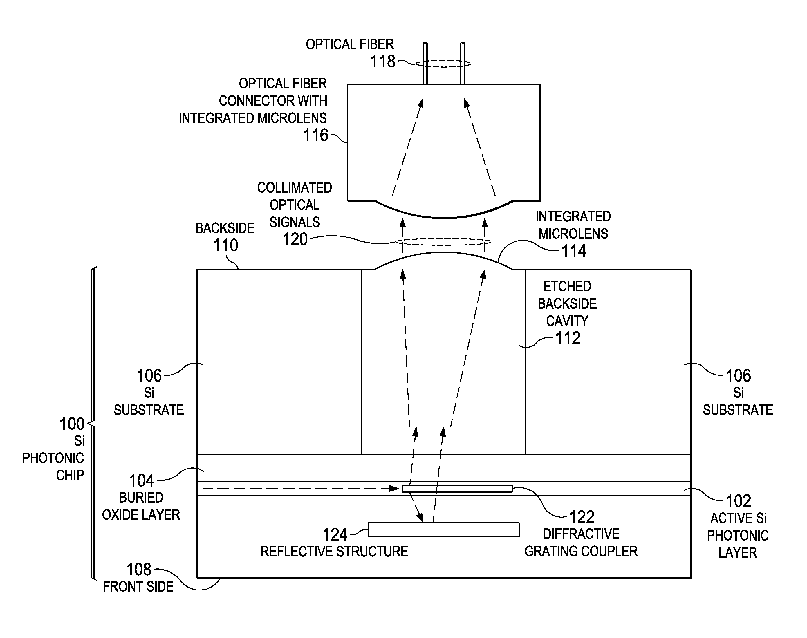
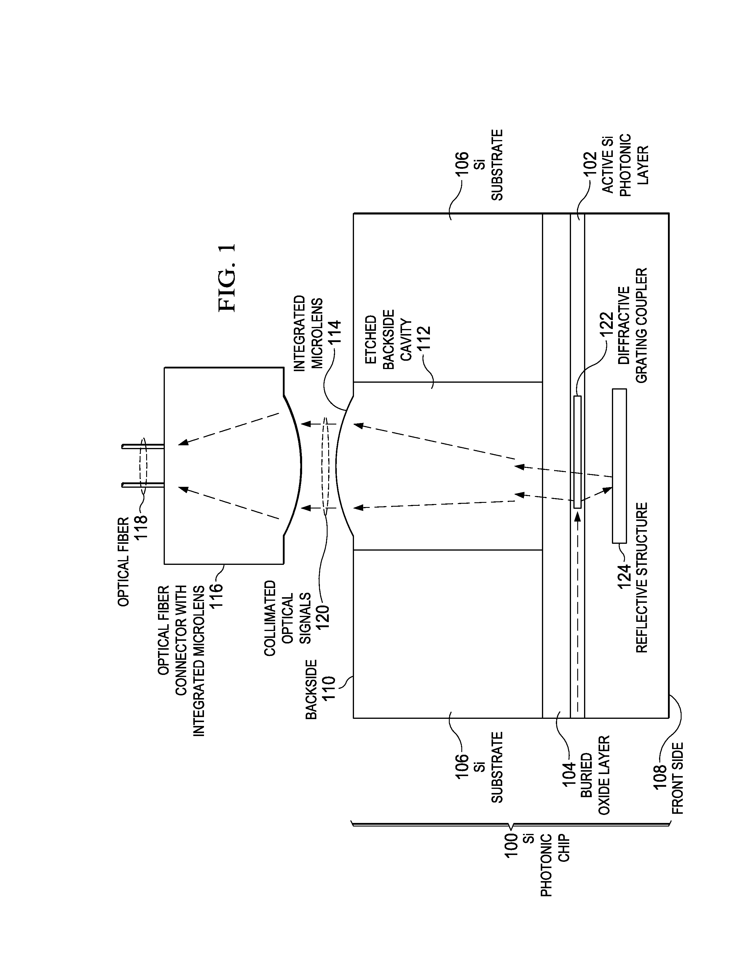
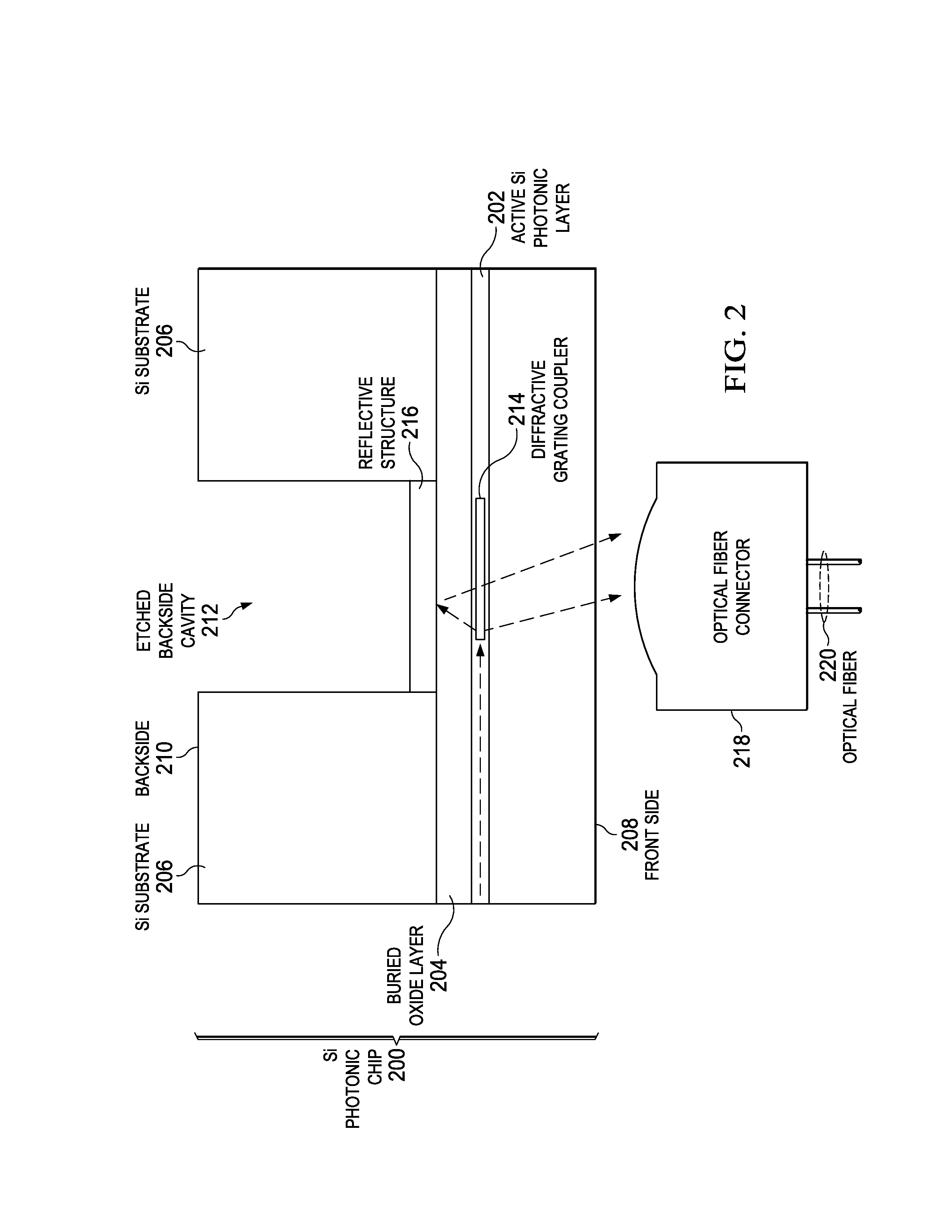
[0011]With reference now to the figures, and in particular, with reference to FIGS. 1-4, diagrams of apparatuses are provided in which illustrative embodiments may be implemented. It should be appreciated that FIGS. 1-4 are only meant as examples and are not intended to assert or imply any limitation with regard to the apparatuses in which different embodiments may be implemented. Many modifications to the depicted apparatuses may be made. In addition, it should be noted that the various features of the figures are not to scale. On the contrary, the dimensions of the various features are arbitrarily expanded or reduced for clarity.

[0012]FIG. 1 depicts a diagram of a cross-section view of a silicon photonic chip with integrated microlens in an etched backside cavity in accordance with an illustrative embodiment. Silicon photonic chip 100 is an example of a semiconductor chip that may be used in a data processing system, such as a computer. In addition, silicon photonic chip 100 is ca...


PUM


Abstract

A silicon photonic chip is provided. An active silicon layer that includes a photonic device is on a front side of the silicon photonic chip. A silicon substrate that includes an etched backside cavity is on a backside of the silicon photonic chip. A microlens is integrated into the etched backside cavity. A buried oxide layer is located between the active silicon layer and the silicon substrate. The buried oxide layer is an etch stop for the etched backside cavity.

Description

BACKGROUND[0001]1. Field[0002]The disclosure relates generally to integrated circuits, silicon chip technology and more specifically to coupling of optical signals to and from a silicon photonic chip.[0003]2. Description of the Related Art[0004]The communication bandwidth between computers and within a computer is playing an increasing role in a system's overall performance. The trend towards multi-core processors and multiple processors per computer requires an increase in communication between processors and between a processor and its memory. Electrical data links perform well over short distances, but electrical data links reach a limit as the link distance and frequency increases. Optical data links over optical fiber are capable of high speed communication with low transmission loss over long distances. However, silicon photonic chips are expensive compared with their electrical counterparts.[0005]Silicon (Si) photonics is a technology that is under worldwide research and deve...

Claims


Application Information

Patent Timeline
IPC IPC(8): G02B6/42G02B6/32
CPCG02B6/4204G02B6/34
Inventor ANDRY, PAUL S.BUDD, RUSSELL A.LIBSCH, FRANK R.WISNIEFF, ROBERT L.
Owner GLOBALFOUNDRIES US INC
Why Eureka
Try Eureka