Silicon photonic chip optical coupling structures

一种硅光子、芯片的技术,应用在光波导的耦合、光学、光学元件等方向,能够解决硅光子芯片昂贵等问题

Inactive Publication Date: 2013-07-24
INT BUSINESS MASCH CORP
View PDF10 Cites 26 Cited by
  • Summary
  • Abstract
  • Description
  • Claims
  • Application Information

AI Technical Summary

Problems solved by technology

However, silicon photonic chips are expensive compared to their electrical counterparts

Method used


Image

  • Silicon photonic chip optical coupling structures
  • Silicon photonic chip optical coupling structures
  • Silicon photonic chip optical coupling structures

Examples


Embodiment Construction

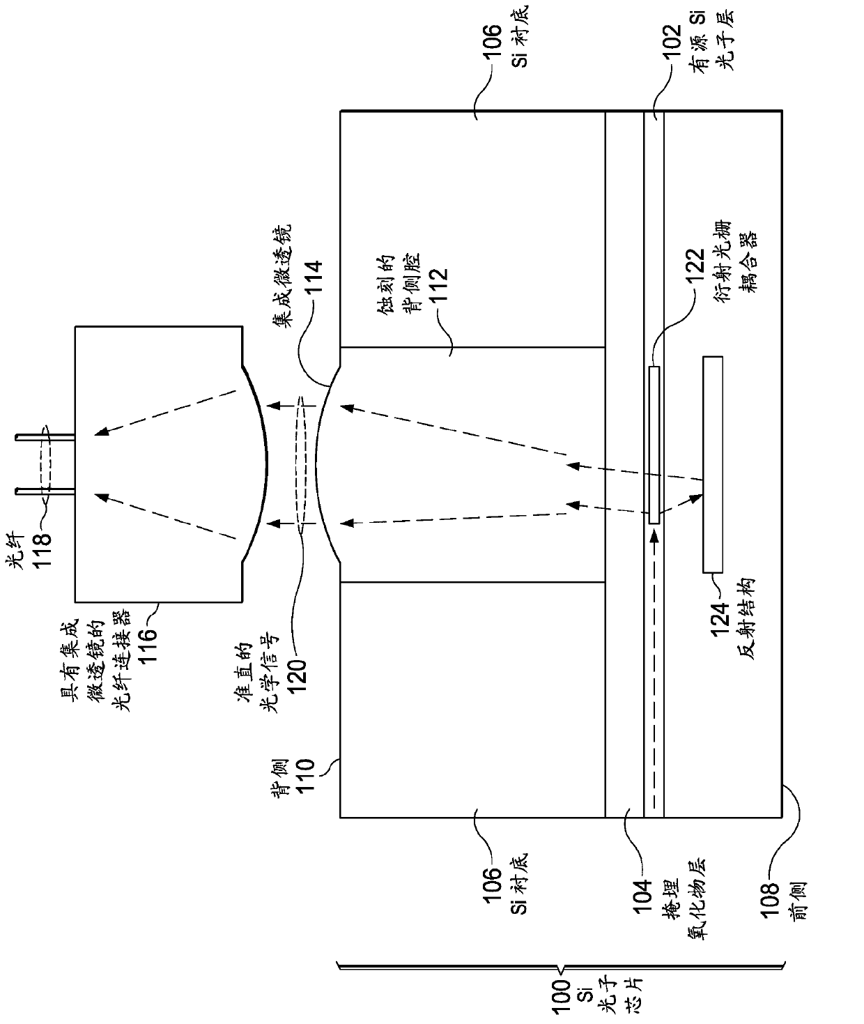
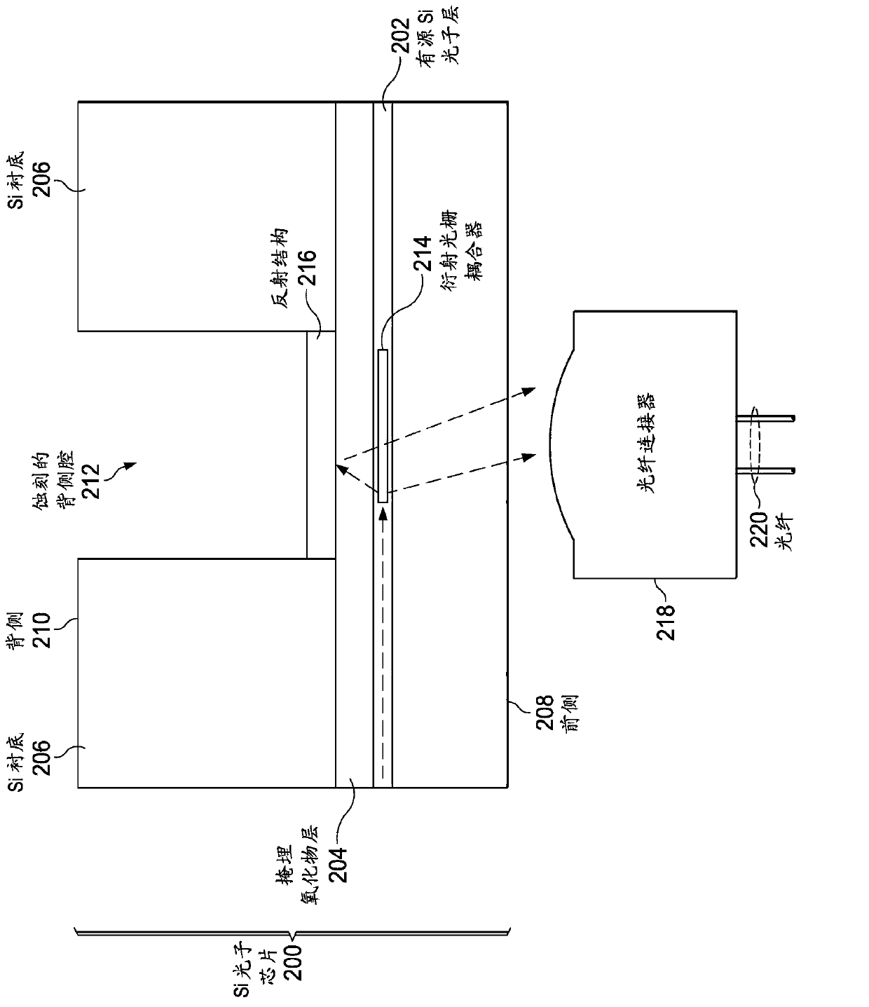
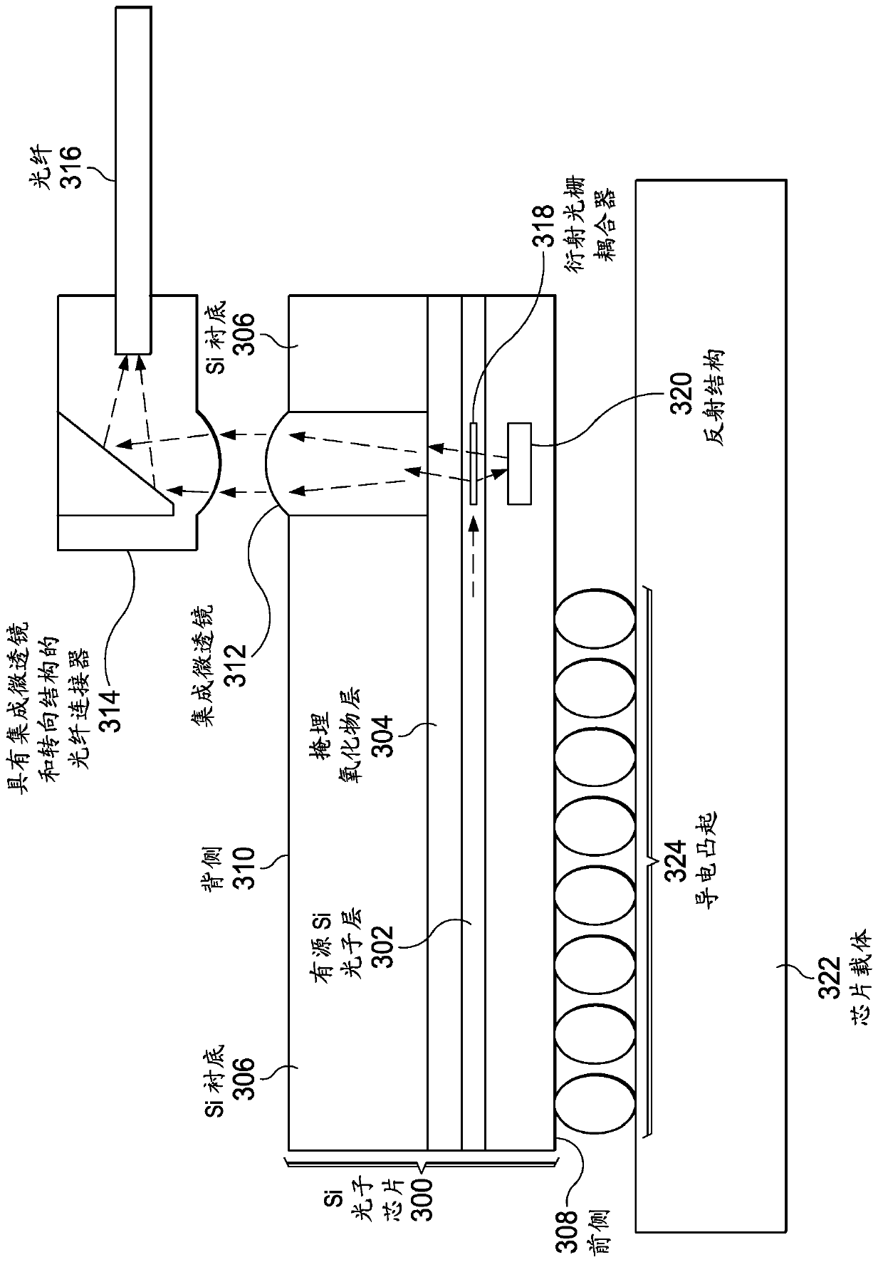
[0009] Referring now to the drawings, specifically, reference Figure 1-4 , Provides a diagram of an apparatus in which the illustrated embodiment can be executed. Should understand, Figure 1-4 Only as an example and not intended to state or imply any limitations on the devices in which different embodiments may be implemented. Many modifications can be made to the described device. In addition, it should be noted that the various features of the drawings are not to scale. On the contrary, for clarity purposes, the size of various features can be enlarged or reduced anywhere.

[0010] figure 1 Shows a cross-sectional view of a silicon photonic chip with integrated microlenses in an etched backside cavity according to the illustrated embodiment; the silicon photonic chip 100 is an example of a semiconductor chip that can be used in a data processing system such as a computer . In addition, the silicon photonic chip 100 can transmit and receive optical signals (ie, light puls...


PUM


Abstract

A silicon photonic chip is provided. An active silicon layer that includes a photonic device is on a front side of the silicon photonic chip. A silicon substrate that includes an etched backside cavity is on a backside of the silicon photonic chip. A microlens is integrated into the etched backside cavity. A buried oxide layer is located between the active silicon layer and the silicon substrate. The buried oxide layer is an etch stop for the etched backside cavity.

Description

Technical field [0001] The present disclosure generally relates to integrated circuit and silicon chip technology, and more specifically, to the coupling of optical signals from silicon photonic chips. Background technique [0002] The communication bandwidth between and among computers plays an important role in the overall performance of the system. The tendency for multi-core processors and multi-level processors in each computer requires an increase in communication between processors and between processors and their memories. The electrical data connection performs well in short distances, but the electrical data connection is limited when the connection distance and frequency increase. The optical data connection on the optical fiber can communicate at a high speed over a long distance with low transmission loss. However, silicon photonic chips are expensive compared to their electrical counterparts. [0003] Silicon (Si) photonics is a technology researched and developed ...

Claims


Application Information

Patent Timeline
Patent Type & Authority Applications(China)
IPC IPC(8): G02B6/122G02B6/42
CPCG02B6/34G02B6/4204
Inventor P·S·安德里R·A·巴德F·R·利布士R·L·威斯涅夫
Owner INT BUSINESS MASCH CORP
Why Eureka
Try Eureka