Hybrid-integrated multi-chip module

a multi-chip module and hybrid technology, applied in the field of multi-chip modules, can solve the problems of difficult to achieve electrically pumped room-temperature continuous-wave (cw) laser in silicon, silicon is usually a poor material for light emission, and light sources on silicon remain a substantial technological challeng

Active Publication Date: 2017-07-13
ORACLE INT CORP
View PDF0 Cites 24 Cited by
  • Summary
  • Abstract
  • Description
  • Claims
  • Application Information

AI Technical Summary

Problems solved by technology

While tremendous progress has been made in developing silicon-on-insulator (SOI) circuits, light sources on silicon remain a substantial technological challenge.
However, because of its indirect bandgap structure, silicon is usually a poor material for light emission.
Although there are ongoing efforts to enhance the light-emitting efficiency and optical gain in silicon, an electrically pumped room-temperature continuous-wave (CW) laser in silicon remains elusive.
Similarly, while there have been exciting developments in the use of germanium directly grown on silicon as the optical gain medium, high-tensile strain and high doping are typically needed to make germanium have a direct bandgap, which usually results in low laser efficiency.
Furthermore, epitaxial growth of III / V compound semiconductors on silicon is often difficult because of the large lattice and thermal mismatches between silicon and the III / V compound semiconductors, which also limits laser efficiency and reliability.
Thus, because of a number of material, process and device physics issues, these areas remain research topics.
However, because of taper loss, carrier-injection efficiency and thermal impedance, these hybrid lasers typically have relatively low optical-waveguide-coupled overall efficiency.
Furthermore, wafer-bonding approaches usually only work for direct bonding of III / V compound semiconductors on a silicon wafer with passive circuits.
In addition, III / V compound-semiconductor wafers and SOI wafers often do not have compatible sizes.
Consequently, integrating hybrid laser sources with other active silicon devices (which may include multiple layers of metal interconnects and interlayer dielectrics) remains a challenge.
However, because of the optical-mode mismatch between the III / V compound-semiconductor and the silicon optical waveguides, special mode size converters on either or both sides of the III / V compound semiconductor and silicon are often needed.
Addressing these problems can decrease the yield and increase the cost of these hybrid lasers.

Method used


Image

  • Hybrid-integrated multi-chip module
  • Hybrid-integrated multi-chip module
  • Hybrid-integrated multi-chip module

Examples


Embodiment Construction

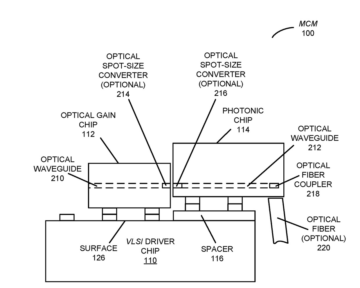
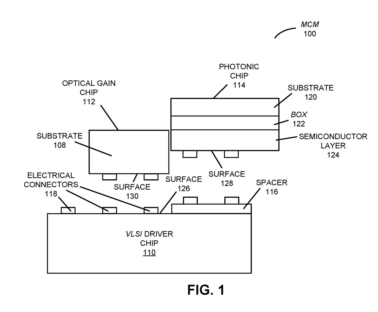
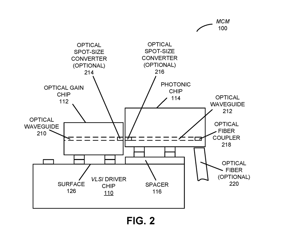
[0035]Embodiments of a multi-chip module (MCM), a system that includes the MCM, and a technique for outputting an optical signal using the MCM are described. This MCM includes a driver integrated circuit that includes electrical circuits, a photonic chip, an interposer, and an optical gain chip. The photonic chip may be implemented using a silicon-on-insulator (SOI) technology, and may include an optical waveguide that conveys an optical signal and traces that are electrically coupled to the driver integrated circuit. Moreover, the interposer may be electrically coupled to the traces. Furthermore, the optical gain chip may include a III / V compound semiconductor (and, more generally, a semiconductor other than silicon), and may include a second optical waveguide that conveys the optical signal and that is vertically aligned with the optical waveguide relative to a top surface of the interposer. Additionally, the optical gain chip may be electrically coupled to the interposer.

[0036]In...


PUM


Abstract

A multi-chip module (MCM) is described. This MCM includes a driver integrated circuit that includes electrical circuits, a photonic chip, an interposer, and an optical gain chip. The photonic chip may be implemented using a silicon-on-insulator technology, and may include an optical waveguide that conveys an optical signal and traces that are electrically coupled to the driver integrated circuit. Moreover, the interposer may be electrically coupled to the traces. Furthermore, the optical gain chip may include a III/V compound semiconductor (and, more generally, a semiconductor other than silicon), and may include a second optical waveguide that conveys the optical signal and that is vertically aligned with the optical waveguide relative to a top surface of the interposer. Additionally, the optical gain chip may be electrically coupled to the interposer.

Description

U.S. GOVERNMENT LICENSE RIGHTS[0001]This invention was made with U.S. Government support under Agreement No. HR0011-08-9-0001 awarded by DARPA. The U.S. Government has certain rights in the invention.BACKGROUND[0002]Field[0003]The present disclosure generally relates to multi-chip modules (MCMs) and techniques for fabricating MCMs. More specifically, the present disclosure relates to an MCM that includes a photonic chip, an interposer and an optical gain chip.[0004]Related Art[0005]Optical interconnects based on silicon-photonics technology have the potential to outperform electrical interconnects in terms of bandwidth, component density, energy efficiency, latency, and physical reach. Consequently, optical interconnects are a promising solution to alleviate inter-chip and intra-chip communication bottlenecks in high-performance computing systems.[0006]While tremendous progress has been made in developing silicon-on-insulator (SOI) circuits, light sources on silicon remain a substan...

Claims


Application Information

Patent Timeline
Patent Type & Authority Applications(United States)
IPC IPC(8): G02B6/122H01S5/022G02B6/42
CPCG02B6/122G02B6/428G02B2006/12147H01S5/0228G02B2006/12121G02B6/1228G02B6/4231G02B6/4274H01S5/0225
Inventor SHUBIN, IVANZHENG, XUEZHELEE, JIN HYOUNGKRISHNAMOORTHY, ASHOK V.
Owner ORACLE INT CORP
Why Eureka
Try Eureka