Semiconductor structure and process thereof

a technology of semiconductors and semiconductors, applied in the direction of resistors, transistors, semiconductor devices, etc., can solve the problems of damage to the structure below the polysilicon, the polysilicon area to remove is difficult to be removed by etching processes, and the metal polishing process is incompl

a technology of semiconductors and semiconductors, applied in the direction of resistors, transistors, semiconductor devices, etc., can solve the problems of damage to the structure below the polysilicon, the polysilicon area to remove is difficult to be removed by etching processes, and the metal polishing process is incompl

US20130200393A1Active Publication Date: 2013-08-08UNITED MICROELECTRONICS CORP

Image

  • Semiconductor structure and process thereof
  • Semiconductor structure and process thereof
  • Semiconductor structure and process thereof

Examples


Embodiment Construction

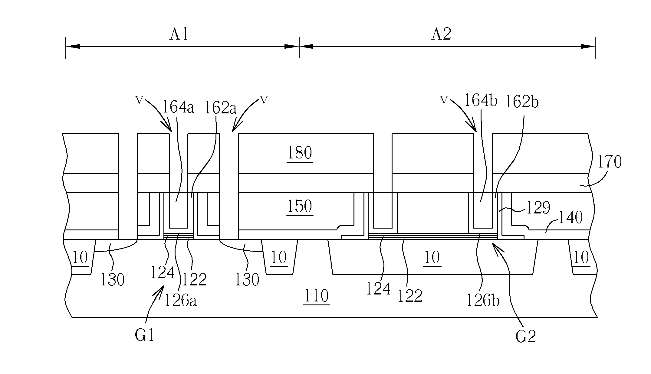
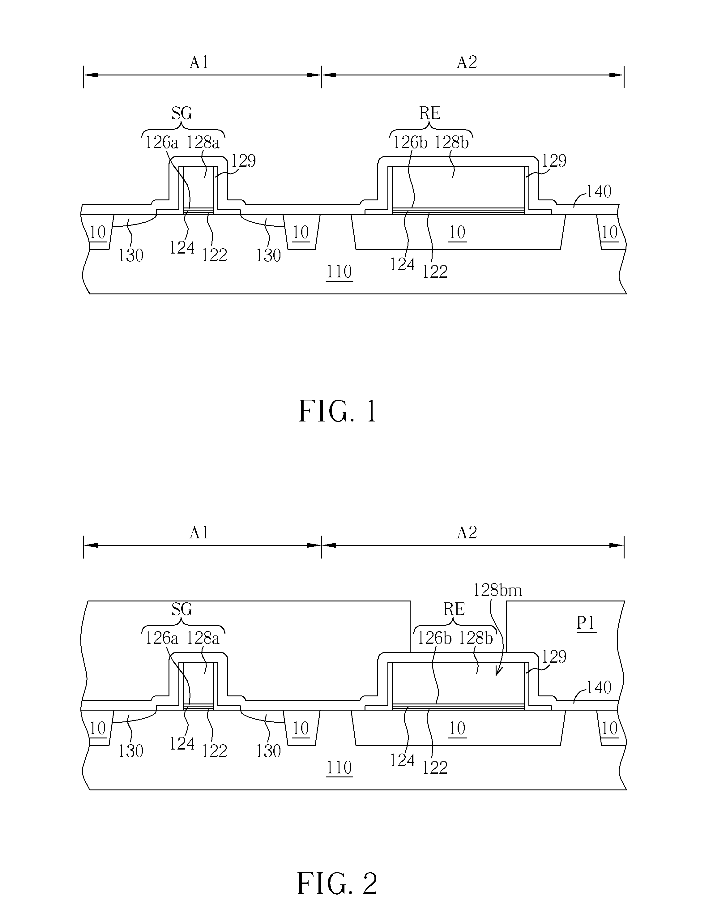
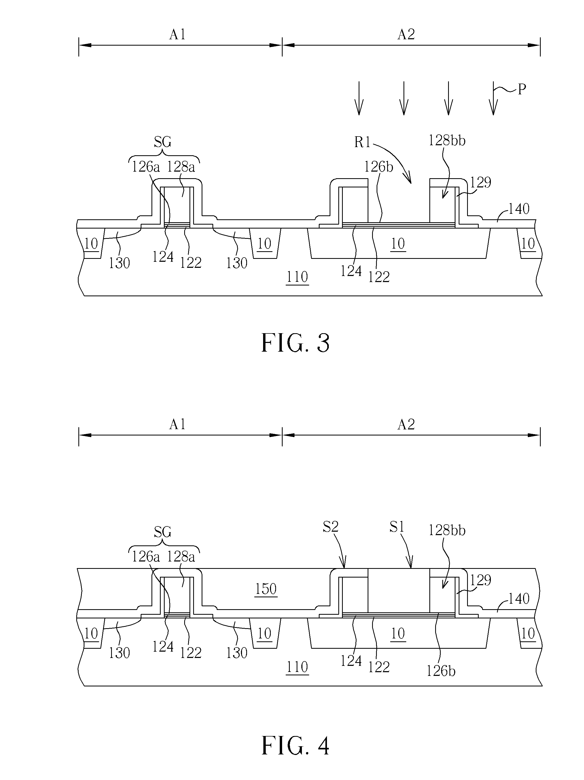
[0013]FIGS. 1-9 schematically depict cross-sectional views of a semiconductor process according to one embodiment of the present invention. As shown in FIG. 1, a substrate 110 having at least an isolation structure 10 is provided. The substrate 10 may be a semiconductor substrate such as a silicon substrate, a silicon containing substrate, an III-V group-on-silicon (such as GaN-on-silicon) substrate, a graphene-on-silicon substrate or a silicon-on-insulator (SOI) substrate. In this embodiment, the isolation structure 10 is a shallow trench isolation structure. In another embodiment, the isolation structure 10 may be a thermal oxidation structure or etc.

[0014]In this embodiment, the substrate 110 is divided into a transistor area and a resist area. A transistor is formed on the substrate 110 of the transistor area and a resistor structure is formed on the substrate 110 of the resist area. The transistor process for forming the transistor and the semiconductor process for forming the ...


PUM

PropertyMeasurementUnit
semiconductoraaaaaaaaaa
dielectric constantaaaaaaaaaa
dielectricaaaaaaaaaa

Abstract

A semiconductor structure includes a substrate, a resist layer, a dielectric material, two U-shaped metal layers and two metals. The substrate has an isolation structure. The resist layer is located on the isolation structure. The dielectric material is located on the resist layer. Two U-shaped metal layers are located at the two sides of the dielectric material and on the resist layer. Two metals are respectively located on the two U-shaped metal layers. This way a semiconductor process for forming said semiconductor structure is provided.

Description

BACKGROUND OF THE INVENTION [0001]1. Field of the Invention[0002]The present invention relates generally to a semiconductor structure and process thereof, and more specifically to a semiconductor structure and process thereof, which includes a resistor structure having two U-shaped metal layers located at the two sides of a dielectric material.[0003]2. Description of the Prior Art[0004]In a semiconductor process, polysilicon is often used in forming resistors capable of providing high resistance. These resistors can be used in place of load transistors. When load transistors of a static random access memory (SRAM) is replaced by polysilicon resistors, the number of transistors in the SRAM can be lowered which reduce costs and enhance the integration ratio of the SRAM.[0005]The steps of forming resistor structures by polysilicon may include covering a silicon nitride layer on a reserved polysilicon area to define a location of a polysilicon resistor by exposing a polysilicon area to ...

Claims


Application Information

Patent Timeline
08 Aug 2013
Publication
US20130200393A1
IPC
H01L29/16; H01L21/28; H10N97/00
CPC
H01L27/0629; H01L21/76897; H01L28/24; H01L29/66545; H01L28/20
Inventors
CHEN, CHIEH-TE; LIN, YI-PO